 |
 |
 |
| Главная Журналы Популярное Audi - почему их так назвали? Как появилась марка Bmw? Откуда появился Lexus? Достижения и устремления Mercedes-Benz Первые модели Chevrolet Электромобиль Nissan Leaf |
Главная » Журналы » Metal oxide semiconductor 1 ... 11 12 13 14 15 16 17 ... 91   7~r 7~r 7  FIGURE 9.15 Cross section of SIT logic. su ly cur ejit out1 out2 out3 9 Q Q FIGURE 9.16 Diagram of SIT logic. 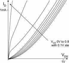 FIGURE 9.17 Measured characteristic of an -channel transistor of the logic circuit of Fig. 9.16. Schottky С 1 Q В о В 6 Е 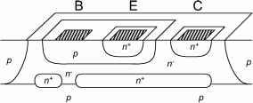 FIGURE 9.19 Cross sections of bipolar transistors protected against deep saturation using SIT. collector capacitance is always enlarged by the Miller effect and this leads to slower switching in the case of the solution with the Schottky diode. 9.10 Static Induction MOS Transistor (SIMOS) The punch-through transistor with MOS controlled gate was described in 1983 [18, 9]. In the structure in Fig. 9.20a current can flow in a similar fashion as in the lateral punch-through transistor [15]. In this mode of operation, carriers are moving far from the surface with a velocity close to saturation. The real advantage of such a structure is the very low gate capacitance. Another implementation of SIMOS is shown in Fig. 9.21. The buried p+-layer is connected to the substrate, which has a 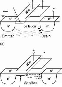 Emitter n Drain FIGURE 9.20 MOS-controUed punch-through transistor: (a) transis-FIGURE 9.18 Protection of a bipolar transistor against deep satura- tor in the punch-through mode for the negative gate potential; and tion: (a) using a Schottky diode; and (b) using SIT. (b) transistor in the on-state for the positive gate potential. im lant 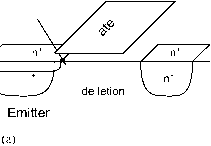 Drain Gate Emitter Drain FIGURE 9.21 (b) top view. Static induction MOS structure: (a) cross section; and large negative potential. As a result the potential barrier is high and the emitter-drain current cannot flow. The punch-through current may start to flow when the positive voltage is applied to the gate and in this way the potential barrier is lowered. The p-implant layer is depleted and due to the high horizontal electrical field under the gate there is no charge accumulation under this gate. Such a transistor has several advantages over the traditional MOS are: 1. The gate capacitance is very smaU because there is no accumulation layer under the gate; 2. carriers are moving with a velocity close to saturation velocity; and 3. much lower substrate doping and the existing depletion layer lead to much smaller drain capacitance. The device operates in a similar fashion as the MOS transistor in subthreshold conditions, but this process occurs at much higher current levels. Such a bipolar mode of operation may have many advantages in VLSI applications. 9.11 Space-Charge Limiting Load (SCLL) Using the concept of the space-charge limited current flow (see Fig. 9.22), it is possible to fabricate very large resistors on a very smaU area. Moreover, these resistors have a very smaU 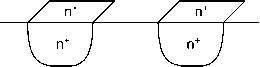 FIGURE 9.22 Space-charge limiting load (SCLL). parasitic capacitance. The 50-kQ resistor requires only several square im using 2-im technology [22]. Depending upon the value of the electric field, the device current is described by the following two equations. For a smaU electrical field v(x) = 1лЕ(х) and for a large electrical field v(x) = const. (9.17) (9.18) Moreover, these resistors, which are based on the space-charge limit flow, have a very smaU parasitic capacitance. 9.12 Power MOS Transistors Power MOS transistors are being used for fast switching power supplies and for switching power converters. They can be driven with relatively smaU power and switching frequencies could be very high. High switching frequencies lead to compact circuit implementations with smaU inductors and smaU capacitances. Basically only two technologies (VMOS and DMOS) are used for power MOS devices as shown in Figs. 9.23 and 9.24, respectively. A more popular structure is the DMOS shown in Fig. 9.24. This structure also uses the static induction transistor concept. Note that for large drain voltages the n-region is depleted from carriers and the statically induced electrical field in the vicinity of the virtual drain is significantly reduced. As a result, this transistor may withstand much larger drain voltages and the effect of channel length modulation also is significantly reduced. The latter effect leads to larger output resistances of the transistor. Therefore, the drain current is less sensitive to source source drain FIGURE 9.23 Cross section of the VMOS transistor. 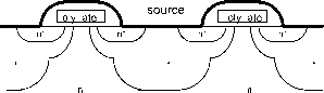 drain FIGURE 9.24 Cross section of the DMOS transistor. drain drain vohage variations. The structure in Fig. 9.24 can be considered as a composite of the MOS transistor and the SIT transistor as it is shown in Fig. 9.25. The major disadvantage of power MOS transistors is their relatively large drain series resistance and much smaller transconductance in comparison to bipolar transistors. Both of these parameters can be improved dramatically by a simple change of the type of drain. In the case of an n-channel device, this change would be from an n-type to a p-type. This way, the integrated structure being built has a diagram of a MOS transistor integrated with a bipolar transistor. Such a structure has P times larger transconductance is the current gain of a bipolar transistor) and much smaller series resistance due to the conductivity modulation effect caused by holes injected into the lightly doped drain region. Such devices are known as insulated gate bipolar transistors (IGBT) as shown in Fig. 9.26. Their main disadvantage is that of large switching time limited primarily by the poor switching performance of the bipolar transistor. Another difficulty is related to a possible latch-up action of four layer -structure. This undesirable effect could be suppressed by using a heavily doped p+-region in the base of the npn structure, which leads to significant reduction of the current gain of this parasitic transistor. The gain of the pnp transistor must be kept large so that the transconductance of the entire device is also large. The IGBTs have breakdown voltages of up to 1500 V and turn-off times in the range of 0.1 9 D G o- FIGURE 9.25 Equivalent diagram with MOS and SI transistors of the structure of Fig. 9.24. 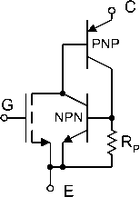 FIGURE 9.26 Insulated gate bipolar transistor (IGBT): (a) cross section; and (b) equivalent diagram. to 0.5 is. They may operate with currents >100A with a forward voltage drop of 3 V. 9.13 Static Induction Thyristor There are several special semiconductor devices dedicated to high-power applications. The most popular is a thyristor known as the silicon control rectifier (SCR). This device has a four-layer structure (Fig 9.27a) and it can be considered as two transistors npn and pnp connected as shown in Fig. 9.27b. In a normal mode of operation (the anode has positive potential) only one junction is reverse biased and it can be represented by capacitance C. A spike of anode voltage can therefore get through capacitor С and it can trigger SRC. This behavior is not acceptable in practical apphcation and therefore as Fig. 9.28 shows a different device structure is being used. Note that shorting the gate to the cathode by resistor R makes it much more difficult to trigger the npn transistor by spike of anode voltage. This way, rapid anode voltage changes are not able to trigger a thyristor. Therefore, this structure has a very large dV/dt parameter. At the same time, much energy anode anode 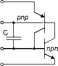 cathode FIGURE 9.27 Silicon control rectifier (SCR): (a) cross section; and (b) equivalent diagram. anode
cathode FIGURE 9.28 Silicon control rectifier (SCR) with larger dV/dt parameter: (a) cross section; and (b) equivalent diagram. is required to trigger the thyristor with the gate signal, which is an undesirable effect and switching on time (described by the di/dt parameter) is lengthy. Most of the SCRs sold on the market consist of an integrated structure composed of two or more thyristors. This structure has both large dV/dt and di/dt parameters. This structure consists of an internal thyristor, which significantly amplifies the gate signal. One can notice that the classical thyristor as shown in Fig. 9.27 can be turned off by the gate voltage while the integrated SCR shown in Fig. 9.29 can only be turned off by reducing anode current to zero. Most of the SCRs sold on the market have an integrated structure composed of two or more thyristors. This structure has both large dV/dt and di/dt parameters. anode У (a) cathode FIGURE 9.29 Integrated structure of silicon control rectifier: (a) cross section; and (b) equivalent diagram. ate -О О О Г cathode FIGURE 9.30 The GTO SITh: (a) cross section; and (b) equivalent diagram. 9.14 Gate Turn-Off Thyristor (GTO) For dc operation it is important to have a thyristor that can be turned off by the gate voltage. Such a thyristor has a structure similar to that shown in Fig. 9.27. It is important, however, to have significantly different current gains P for pnp and npn transistors. The current gain of an npn transistor should be as large as possible and the current gain of a pnp transistor should be smaU. The product of and fpp should be larger than unity. This can be easily implemented using the SI structure as shown in Fig. 9.30. References 1. Baliga, B. J. The pinch rectifier: A low forward-drop, high-speed power diode, IEEE Electron Device Letters 5: 194-196 (1984). 2. Kim, C. W., M. Kimura, K. Yano, A. Tanaka, and T. Sukegawa, Bipolar-mode static induction transistor: Experiment and two-dimensional analysis, IEEE Trans. Electron Devices 37:9, 2070-2075 (1990). 3. Lewandowski, D. and B. M. Wilamowski, On the dynamic properties of SITL inverter, Electron Technology 14:3/4, 19-26 (1981). 4. Mattson, R. H. and B. M. Wilamowski, Punch-Through Devices Operating in Space-Charge-Limited Modes, IEEE International Workshop on the Physics of Semiconductor Devices, Delhi, India, December 5-10, 1983. 5. Nakamura, Y., H. Tadano, M. Takigawa, I. Igarashi, and J. Nishizawa, Experimental Study on Current Gain of BSIT, IEEE Trans. Electron Devices 33:6, 810-815 (1986). 6. Nishizawa, J., T. Ohmi, and H. L. Chen, Analysis of static characteristics of a bipolar-mode SIT (BSIT), IEEE Trans. Electron Devices 29:8, 1233-1244 (1982). 7. Nishizawa, J., T. Terasaki, and J. Shibata, Field-effect transistor versus analog transistor (static induction transistor), IEEE Trans. Electron Devices 22:4, 185-197 (1975). 8. Nishizawa, J. and B. M. Wilamowski, Integrated Logic - State Induction Transistor Logic, International Solid State Circuit Conference, Philadelphia USA, 1977, pp. 222-223. 9. Nishizawa, J. and B. M. Wilamowski, Static Induction Logic - A Simple Structure with Very Low Switching Energy and Very High Packing Density, International Conference on Solid State Devices, Tokyo, Japan, pp. 53-54, 1976; Jour. Japanese Soc. Appl. Physics 16-1, 158-162 (1977). 10. Ohmi, Т., Punching through device and its integration - static induction transistor, IEEE Trans. Electron Devices 27, 536-545 (1980). 11. Plotka, P. and B. M. Wilamowski, Interpretation of exponential type drain characteristics of the SIT, Solid-State Electronics 23, 693-694 (1980). 12. Plotka, P. and B. M. Wilamowski, Temperature properties of the static induction transistor, Solid-State Electronics 24, 105-107 (1981). 13. Shimizu, Y., M. Naito, S. Murakami, and Y. Terasawa, High-speed low-loss p-n diode having a channel structure, IEEE Trans. Electron Devices 31:9, 1314-1319 (1984). 14. Stork, J. M. C. and J. D. Plummer, Small geometry depleted barrier bipolar transistor (BSIT), IEEE Trans. Electron Devices 29, 1354-1363 (1982). 15. Wilamowski, B. M. and R. C. Jaeger, The lateral punch-through transistor, IEEE Electron Device letters 3:10, 277-280 (1982). 16. Wilamowski, B. M. and T. J. Englert, CMT - conductivity modulated transistor, IEEE Trans. Electron Devices 39:11,2600-2606 (1992). 17. Wilamowski, B. M., Schottky diodes with high breakdown voltage, Solid-State Electronics 26:5, 491-493 (1983). 18. Wilamowski, B. M., The punch-through transistor with MOS controlled gate, Phys. Status Solidi (a) 79, 631-637 (1983). 19. Wilamowski, B. M., R. C. Jaeger, and J. N. Fordemwalt, Buried MOS transistor with punch-through, Solid State Electronics 27:8/9, 811-815 (1984). 20. Wilamowski, B. M., R. H. Mattson, and Z. J. Staszak, The SIT saturation protected bipolar transistor, IEEE Electron Device letters 5, 263-265 (1984). 21. Wilamowski, B. M., Z. J. Staszak, and R. H. Mattson, An electrical network approach to the analyses of semiconductor devices, IEEE Trans. Education 35:2, 144-152 (1992). 22. Wilamowski, B. M., R. H. Mattson, Z. J. Staszak, and A. Musallam, Punch-through space-charge limited loads, IEEE Electronic Component Conference, Seattle, Washington, USA, pp. 399-404, May 5-7, 1986. 23. Yano, K., I. Henmi, M. Kasuga, and A. Shimizu, High-power rectifier using the BSIT operation, IEEE Trans. Electron Devices 45:2, 563-565 (1998). 24. Yano, K., M. Masahito, H. Moroshima, J. Morita, M. Kasuga, and A. Shimizu, Rectifier characteristics based on bipolar-mode SIT operation, IEEE Electron Device letters 15:9, 321-323 (1994). Diode Rectifiers Yim-Shu Lee, Ph.D. and Martin H. L. Chow, Ph.D. Department of Electronic and Information Engineering The Hong Kong Polytechnic University, Hung Нот, Hong Kong 10.1 Introduction...................................................................................... 139 10.2 Single-Phase Diode Rectifiers................................................................ 139 10.2.1 Single-Phase Half-Wave Rectifiers 10.2.2 Single-Phase Full-Wave Rectifiers 10.2.3 Performance Parameters 10.2.4 Design Considerations 10.3 Three-Phase Diode Rectifiers................................................................ 144 10.3.1 Three-Phase Star Rectifiers 10.3.2 Three-Phase Bridge Rectifiers 10.3.3 Operation of Rectifiers with Finite Source Inductance 10.4 Poly-Phase Diode Rectifiers.................................................................. 148 10.4.1 Six-Phase Star Rectifier 10.4.2 Six-Phase Series Bridge Rectifier 10.4.3 Six-Phase Parallel Bridge Rectifier 10.5 Filtering Systems in Rectifier Circuits..................................................... 150 10.5.1 Inductive-Input dc Filters 10.5.2 Capactive-Input dc Filters 10.6 Fiigh-Frequency Diode Rectifier Circuits................................................ 154 10.6.1 Forward Rectifier Diode, Flywheel Diode, and Magnetic-Reset Clamping Diode in a Forward Converter 10.6.2 Flyback Rectifier Diode and Clamping Diode in a Flyback Converter 10.6.3 Design Considerations 10.6.4 Precautions in Interpreting Simulation Results References......................................................................................... 168 10.1 Introduction This chapter is concerned with the application and design of diode rectifier circuits. It covers single-phase, three-phase, poly-phase and high-frequency rectifier circuits [1, 2]. The objectives of this chapter are: To enable readers to understand the operation of typical rectifier circuits. To enable readers to appreciate the different qualities of rectifiers required for different applications. To enable the reader to design practical rectifier circuits. The high-frequency rectifier waveforms given are obtained from PSpice simulations, [3-5] which take into account the secondary effects of stray and parasitic components. In this way, these waveforms will closely resemble real waveforms. These waveforms are particularly useful to help designers determine the practical voltage, current, and other ratings of high-frequency rectifiers. 10.2 Single-Phase Diode Rectifiers There are two types of single-phase diode rectifier that convert a single-phase ac supply into a dc voltage, namely, single-phase half-wave rectifiers and single-phase full-wave rectifiers. In the following subsections, the operations of these rectifier circuits are examined and their performances are analyzed and compared in tabular form. For the sake of simplicity the diodes are considered to be ideal, that is, they have zero forward voltage drop and reverse recovery time. This assumption is generally valid for the case of diode rectifiers that use the mains, a low-frequency source, as the input, and when the forward voltage drop is small compared with the peak voltage of the mains. Furthermore, it is assumed that the load is purely resistive such that load voltage and load current have similar waveforms. In Section 10.5 the effects of both inductive and capacitive load on a diode rectifier are considered in detail. 10.2.1 Single-Phase Half-Wave Rectifiers The simplest single-phase diode rectifier is the single-phase half-wave rectifier. A single-phase half-wave rectifier with resistive load is shown in Fig. 10.1. The circuit consists of only one diode that is usually fed with a transformer secondary as shown. During the positive half-cycle of the transformer secondary voltage, diode D conducts. During the negative half-cycle, diode D stops conducting. Assuming that the transformer has zero internal impedance and provides perfect sinusoidal voltage on its secondary winding, the voltage and  -I>l- v=V sin cut FIGURE 10.1 A single-phase half-wave rectifier with resistive load. current waveforms of resistive load R and the voltage waveform of diode D are shown in Fig. 10.2. By observing the voltage waveform of diode D in Fig. 10.2, it is clear that the peak inverse voltage (PIV) of diode D is equal to during the negative half-cycle of the transformer secondary voltage. Hence the Peak Repetitive Reverse Voltage ( Vjrm) rating of diode D must be chosen to be higher than to avoid reverse breakdown. In the positive half-cycle of the transformer secondary voltage, diode D has a forward current which is equal to the load current and, therefore, the Peak Repetitive Forward Current (4rm) rating of diode D must be chosen to be higher than the peak load current V/i, in practice. In addition, the transformer has to carry a dc current that may result in a dc saturation problem of the transformer core. 10.2.2 Single-Phase Full-Wave Rectifiers There are two types of single-phase fuU-wave rectifier, namely, fuU-wave rectifiers with center-tapped transformer and bridge rectifiers. A fuU-wave rectifier with a center-tapped transformer is shown in Fig. 10.3. It is clear that each diode, together
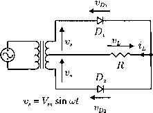 FIGURE 10.3 Full-wave rectifier with center-tapped transformer. with the associated half of the transformer, acts as a half-wave rectifier. The outputs of the two half-wave rectifiers are combined to produce fuU-wave rectification in the load. As far as the transformer is concerned, the dc currents of the two half-wave rectifiers are equal and opposite, such that there is no dc current for creating a transformer core saturation problem. The voltage and current waveforms of the fuU-wave rectifier are shown in Fig. 10.4. By observing diode 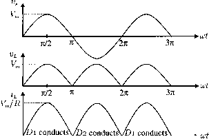 FIGURE 10.2 Voli with resistive load.
with center-tapped transformer. voltage waveforms Vji and Vj2 FB- l-? it is clear that the peak inverse voltage (PIV) of the diodes is equal to 2 during their blocking state. Hence the Peak Repetitive Reverse Voltage ( Vrrm) rating of the diodes must be chosen to be higher than 2V to avoid reverse breakdown. (Note that, compared with the half-wave rectifier shown in Fig. 10.1, the full-wave rectifier has twice the dc output voltage, as shown in Section 10.2.4.) During its conducting state, each diode has a forward current that is equal to the load current and, therefore, the Peak Repetitive Forward Current (/ркм) rating of these diodes must be chosen to be higher than the peak load current Vy/R in practice. Employing four diodes instead of two, a bridge rectifier as shown in Fig. 10.5 can provide full-wave rectification without using a center-tapped transformer. During the positive half-cycle of the transformer secondary voltage, the current flows to the load through diodes D\ and D2. During the negative half cycle, D3 and DA conduct. The voltage and current waveforms of the bridge rectifier are shown in Fig. 10.6. As with the full-wave rectifier with center-tapped transformer, the Peak Repetitive Forward Current (/ркм) rating of the employed diodes must be chosen to be higher than the peak load current Vm/R However, the peak inverse voltage (PIV) of the diodes is reduced from 2V to during their blocking state.
FIGURE 10.6 Voltage and current waveforms of the bridge rectifier. 10.2.3 Performance Parameters In this section the performance of the rectifiers mentioned in the preceding will be evaluated in terms of the following parameters. angular frequency of the source ш = 2я/Т, and Eq. (10.1) can be rewritten as sm(Dtd{(Dt) (10.2) 10.2.3.1 Voltage Relationships The average value of the load voltage Vi is V and it is defined as Therefore, Half-wave V = = 0.318 V (10.3) Vr{t)dt (10.1) In the case of a half-wave rectifier. Fig. 10.2 indicates that load voltage Vi{t) = 0 for the negative half-cycle. Note that the In the case of a full-wave rectifier. Figs. 10.4 and 10.6 indicate that Viit) = I sin cot I for both the positive and negative half-cycles. Hence Eq. (10.1) can be rewritten as dc=- V sm <X)t d(a)t) (10.4) = sin ijot FIGURE 10.5 Bridge rectifier. Therefore, Full-wave Vj, = -- = 0.636 (10.5) L The root-mean-square (rms) value of load voltage Vi is V, which is defined as T nl/2 viit)dt (10.6) In the case of a half-wave rectifier, Vi(t) = 0 for the negative half-cycle, therefore, Eq. (10.6) can be rewritten as r=lj (V sin (Dtfd((Dt) Half-wave = = 0.5 (10.7) (10.8) In the case of a fuU-wave rectifier, Vi(t) = Vsina;t for both the positive and negative half-cycles. Hence, Eq. (10.6) can be rewritten as (V sin CDtfd(cDt) (10.9) Full-wave Vr = = 0.707 (10.10) The result of Eq. (10.10) is as expected because the rms value of a full-wave rectified voltage should be equal to that of the original ac voltage. 10.2.3.2 Current Relationships The average value of load current ii is L and because load R is purely resistive it can be found as (10.11) The root-mean-square (rms) value of load current ii is 7 and it can be found as In the case of a half-wave rectifier, from Eq. (10.3) 0.318 Half-wave L = and from Eq. (10.8) Half-wave = II = In the case of a fuU-wave rectifier, from Eq. (10.5) 0.636 FuU-wave L = (10.12) (10.13) (10.14) (10.15) and from Eq. (10.10) FuU-wave L = (10.16) 10.2.3.3 Rectification Ratio The rectification ratio, which is a figure of merit for comparing the effectiveness of rectification, is defined as (10.17) In the case of a half-wave diode rectifier, the rectification ratio can be determined by substituting Eqs. (10.3), (10.13), (10.8), and (10.14) into Eq. (10.17). Half-wave. = -Y = 40.50/ (0.5 Vj (10.18) In the case of a fuU-wave rectifier, the rectification ratio is obtained by substituting Eq. (10.5), (10.15), (10.10), and (10.16) into Eq. (10.17). Full-wave a = (0.707 Vj (10.19) 10.2.3.4 Form Factor The form factor (FF) is defined as the ratio of the root-mean-square value (heating component) of a voltage or current to its average value. FF = or - (10.20) In the case of a half-wave rectifier, the FF can be found by substituting Eqs. (10.8) and (10.3) into Eq. (10.20) Half-wave FF = = 1.57 (10.21) 0.318 In the case of a fuU-wave rectifier, the FF can be found by substituting Eqs. (10.16) and (10.15) into Eq. (10.20) FuU-wave FF = = 1.11 (10.22) 0.636 10.2.3.5 Ripple Factor The ripple factor (RF), which is a measure of the ripple content, is defined as RF = (10.23) 1 ... 11 12 13 14 15 16 17 ... 91 |
|||||||||||||||||||||||||||||||||||||||||||||||||||||||||||||||||||||||||||||||||||||||||||||||||||||||||||||||||||||||||||||||||
|
© 2026 AutoElektrix.ru
Частичное копирование материалов разрешено при условии активной ссылки |