 |
 |
 |
| Главная Журналы Популярное Audi - почему их так назвали? Как появилась марка Bmw? Откуда появился Lexus? Достижения и устремления Mercedes-Benz Первые модели Chevrolet Электромобиль Nissan Leaf |
Главная » Журналы » Metal oxide semiconductor 1 ... 13 14 15 16 17 18 19 ... 91 TABLE 10.5 Important design parameters of typical rectifier circuits with inductor-input dc filter
shown in Fig. 10.27. When the instantaneous voltage of the secondary winding is higher than the instantaneous value of capacitor voltage Vi, either D or D2 conducts, and capacitor С is charged up from the transformer. When the instantaneous voltage of the secondary winding falls below the instantaneous value of capacitor voltage Vi, both diodes are reverse biased and capacitor С is discharged through load resistance R. The resulting capacitor voltage Vi varies between a maximum value of and a minimum value of - V(pp) as shown in Fig. 10.27. (V(pp) is the peak-to-peak ripple voltage.) As shown in Fig. 10.27, the conduction angle 6 of the diodes becomes smaller when the output ripple voltage decreases. Consequently, the power supply and diodes suffer from high repetitive surge currents. An LC ac filter, as shown in Fig. 10.24, may be required to improve the input power factor of the rectifier. In practice, if the peak-to-peak ripple voltage is small, it can be approximated as r(pp) - frRC (10.77) where is the output ripple frequency of the rectifier. inrush -► -t>b- Therefore, the average output voltage V is given by (10.78) 2f,RC The rms output ripple voltage V is approximated by у = - (10.79) The ripple factor RF can be found from RF = V2(2f,RC - 1) 71/2 n Di conducts In 3k Di conducts (10.80) r(pp) 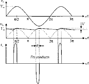 FIGURE 10.26 Full-wave rectifier with capacitor-input dc filter. FIGURE 10.27 Voltage and current waveforms of the full-wave rectifier with capacitor-input dc filter. 10.5.2.1 Inrush Current The resistor iinmsh FB- 10-26 is used to hmit the inrush current imposed on the diodes during the instant the rectifier is being connected to the supply. The inrush current can be very large because capacitor С initially has zero charge. The worst case occurs when the rectifier is connected to the supply at its maximum voltage. The worst-case inrush current can be estimated fi-om -inrush sec + ] (10.81) where R is the equivalent resistance looking from the transformer secondary and equivalent series resistance (ESR) of the filtering capacitor is iESR- Hence, the employed diode should be able to withstand the inrush current for a half-cycle of the input voltage. In other words, the Maximum Allowable Surge Current (/рзм) rating of the employed diodes must be higher than the inrush current. The equivalent resistance associated with the transformer windings and the filtering capacitor is usually sufficient to limit the inrush current to an acceptable level. However, in cases where the transformer is omitted, for example, the rectifier of an off-line switch-mode supply, resistor iinmsh niust be added for controlhng inrush current. Consider as an example a single-phase bridge rectifier, which is to be connected to a 120-V 60-Hz source (without transformer). Assume that the Maximum Allowable Surge Current (/р8м) rating of the diodes is 150 A for an interval of 8.3 ms. If the ESR of the filtering capacitor is zero, we estimate from Eq. (10.81) that the value of the resistor for limiting inrush current resistance is 1.13 Q. 10.6 High-Frequency Diode Rectifier Circuits In high-frequency converters, diodes perform various functions, such as rectifying, flywheeling, and clamping. One special quality a high-frequency diode must possess is a fast switching speed. In technical terms, it must have a short reverse recovery time and a short forward recovery time. The reverse recovery time of a diode may be understood as the time a forwardly conducting diode takes to recover to a blocking state when the voltage across it is suddenly reversed (which is known as forced turn-off). The temporary short circuit during the reverse recovery period may result in large reverse current, excessive ringing, and large power dissipation, aU of which are highly undesirable. The forward recovery time of a diode may be understood as the time a nonconducting diode takes to change to the fully on state when a forward current is suddenly forced into it (which is known as forced turn-on). Before the diode reaches the fully on state, the forward voltage drop during the forward recovery time can be significantly higher than the normal on-state voltage drop. This may cause voltage spikes in the circuit. It should be interesting to note that, as far as circuit operation is concerned, a diode with a long reverse recovery time is similar to a diode with a large parasitic capacitance. A diode with a long forward recovery time is similar to a diode with a large parasitic inductance. (Spikes caused by the slow forward recovery of diodes are often wrongly thought to be caused by leakage inductance.) Comparatively, the adverse effect of a long reverse recovery time is much worse than that of a long forward recovery time. Among commonly used diodes, the Schottky diode has the shortest forward and reverse recovery times. Schottky diodes are therefore most suitable for high-frequency applications. However, Schottky diodes have relatively low reverse breakdown voltage (normally lower than 200 V) and large leakage current. If, due to these limitations, Schottky diodes cannot be used, ultra-fast diodes should be used in high-frequency converter circuits. Using the example of a forward converter, the operations of a forward rectifier diode, a flywheel diode, and a clamping diode wiU be studied in Section 10.6.1. Because of the difficulties encountered in fuU analyses when taking into account parasitic/stray/leakage components, PSpice simulations are extensively used here to study the foUowing [3-5]: The ideahzed operation of the converter; the adverse effects of relatively slow rectifiers (e.g., the so-called ultra-fast diodes, which are actually much slower than Schottky diodes); the improvement achievable by using high-speed rectifiers (Schottky diodes); the effects of leakage inductance of the transformer; the use of snubber circuits to reduce ringing; and the operation of a practical converter with snubber circuits. Using the example of a flyback converter, the operations of a flyback rectifier diode and a clamping diode also will be studied in Section 10.6.2. The design considerations for high-frequency diode rectifier circuits wiU be discussed in Section 10.6.3. The precautions that must be taken in the interpretation of computer simulation results are briefly discussed in Section 10.6.4. 10.6.1 Forward Rectifier Diode, Flywheel Diode, and Magnetic-Reset Clamping Diode in a Forward Converter 10.6.1.1 Ideal Circuit Fig. 10.28 shows the basic circuit of a forward converter. Fig. 10.29 shows the idealized steady-state waveforms for continuous-mode operation (the current in L is continuous). These waveforms are obtained from PSpice simulations, based on the following assumptions: 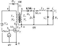 given by FIGURE 10.28 Basic circuit of forward converter. Note that: Fin = 50 V; Li = 8 iH; q = 300 iF; Lp = 0.576 mH; = 0.576 mH; Ls = О.ОЗбтН; = 0.35 Q; and Л^р : Л^ : Л^ = 4 : 4 : 1. Rectifier diode Dj, flywheel diode Dp, and magnetic-reset clamping diode D are ideal diodes with infinitely fast switching speed. Electronic switch is an idealized MOS switch with infinitely fast switching speed, with on-state resistance of 0.067 Q, and off-state resistance of 1 MQ. It should be noted that PSpice does not allow a switch to have zero on-state resistance and infinite off-state resistance. Transformer has a coupling coefficient of 0.99999999. The PSpice program does not accept a coupling coefficient of 1. The switching operation of the converter has reached a steady state. Referring to the circuit shown in Fig. 10.28 and the waveforms shown in Fig. 10.29, the operation of the converter can be explained as follows: 1. For 0 < t < DT (D is the duty cycle of the MOS switch Ml and T is the switching period of the converter, is turned on when Vl(VPULSE) is 15 V, and turned off when Vl(VPULSE) is OV.) The switch is turned on at t = 0. The vohage at node 3, denoted as V(3), is V(3) = 0 for 0 <t <DT (10.82) The voltage induced at node 6 of the secondary wind- ing Ls V(6) = VNs/Np) (10.83) This voltage drives a current I(DR) (current through rectifier diode Dp) into the output circuit to produce the output voltage V. The rate of increase of I(DR) is I(DR) dt -vA- (10.84) where is the dc output voltage of the converter. The flywheel diode Dp is reversely biased by V(9), the voltage at node 9 V(9) = Vi(Ns/Np) for 0<t<DT (10.85) The magnetic-reset clamping diode D is reversely biased by the negative voltage at node 100. Assuming that and Lp have the same number of turns, we have V(100) = -yiN for 0<t<DT (10.86) A magnetizing current builds up linearly in Lp. This magnetizing current reaches the maximum value of (ViDT)/Lp at t = DT. 2. For DT <t < 2DT The switch is turned off at t = DT. The collapse of magnetic flux induces a back emf in L, which is equal to Lp, to turn on the clamping diode D. The magnetizing current in L drops (from the maximum value of {yiDT)/Lp, as mentioned in the preceding) at the rate of Vi/Lp. It reaches zero at t = 2DT. The back emf induced across Lp is equal to Уц. The voltage at node 3 is V(3) = 2 for DT < t < 2DT (10.87) The back emf across Lg forces Dp to stop conducting. The inductive current in L forces the flywheel diode Dp to conduct. Fiere I(Li) (current through L) falls at the rate of di(u)-v, dt Li (10.88) The voltage across Dp, denoted as V(6, 9) (the voltage at node 6 with respect to node 9), is V(DR) = V(6, 9) = -Vi(Ns/Np) for DT <t < 2DT (10.89) 3. For 2DT <t <T Fiere Dj stops conducting at t = 2DT. The voltage across Lj then falls to zero. □ Vl(VPULSE) □ I(DM) -5.0A □ ID(Ml) lOOV -lOOV 200V OV -200V □ V(IOO) □ V(3) -20V □ V(6) -20V □ V(9) 20V OV -20V □ V(6,9) OA -20A 20A OA -20A □ I(DR) □ I(DF) □ I(L1) 5.1V 5.0V 4 4.9V □ V(99) 4us 5us DT lOus T 15us Time 20us FIGURE 10.29 Idealized steady-state waveforms of forward converter for continuous-mode operation. 500mA OA -500mA 5.0A The voltage across Lp is zero V(3) = (10.90) The vohage across L is also zero V(6) = 0 (10.91) Inductive current I(Li) continues to fall at the rate of JPIZX. (10.92) at Li The switching cycle restarts when the switch is turned on again at t = T. From the waveforms shown in Fig. 10.29, the following useful information (for continuous-mode operation) can be found: The output voltage is equal to the average value of V(9), (10.93) The maximum current in the forward rectifying diode Dp and flywheel diode Dp is I(DR) = I(DE) = 4+(l-D)T (10.94) Z Li where = DVi(Ns/Np) and is the output loading current. The maximum reverse voltage of Dp and Dp is V(DR) =V(DF) = V(6,9) = y,n (10.95) The maximum reverse voltage of Dj is V(DM) = V, The maximum current in Dj is I(DM) = DT (10.96) (10.97) The maximum current in the switch M, denoted as ID(Mi), is ID(Mi)ax=TI(DRLax + I(DM) Mp Lp (10.98) Fiowever, it should be understood that, due to the nonideal characteristics of practical components, the idealized wave- forms shown in Fig. 10.29 cannot actually be achieved in the real world. In the following, the effects of nonideal diodes and transformers will be examined. 10.6.1.2 Circuit Using Ultra-Fast Diodes Fig. 10.30 shows the waveforms of the forward converter (circuit given in Fig. 10.28) when ultra-fast diodes are used as D, Dp, and Dp. (Note that ultra-fast diodes are actually much slower than Schottky diodes.) The waveforms are obtained by PSpice simulations, based on the following assumptions: D is an MUR460 ultra-fast diode, and Dp and Dp are MUR1560 ultra-fast diodes; Ml is an IRF640 MOS transistor; transformer has a couphng coefficient of 0.99999999 (which may be assumed to be 1); and the switching operation of the converter has reached a steady state. It is observed that a large spike appears in the current waveforms of diodes Dp and Dp (denoted as I(DR) and I(DF) in Fig. 10.30) whenever the MOS transistor is turned on. This is due to the relatively slow reverse recovery of the flywheel diode Dp. During the reverse recovery time, the positive voltage suddenly appearing across L (which is equal to Vi(Ns/Np)) drives a large transient current through Dp and Dp. This current spike results in large current stress and power dissipation in Dp, Dp, and M. A method of reducing the current spikes is to use Schottky diodes as Dp and Dp, as will be described in what follows. 10.6.1.3 Circuit Using Schottky Diodes In order to reduce the current spikes caused by the slow reverse recovery of rectifiers, Schottky diodes are now used as Dp and Dp. The assumptions made here are (referring to the circuit shown in Fig. 10.28): Dp and Dp are MBR2540 Schottky diodes; Dm is an MUR460 uhra-fast diode; Ml is an IRF640 MOS transistor; transformer has a coupling coefficient of 0.99999999; and the switching operation of the converter has reached a steady state. The new simulated waveforms are given in Fig. 10.31. It is found that when Schottky diodes are used as Dp and Dp, the amplitudes of the current spikes in ID(Ml), I(DR), and I(DF) can be reduced to practically zero. This solves the slow-speed problem of ultra-fast diodes. 10.6.1.4 Circuit with Practical Transformer The simulation results given in Figs. 10.29-10.31 (for the forward converter circuit shown in Fig. 10.28) are based on □ Vl(VPULSE) 500mA -500mA □ I(DM) -40A □ ID(Ml) lOOV -lOOV 200V □ V(IOO) -200V □ V(3) -20V □ V(6) -20V □ V(9) -20V □ V(6,9 lOOA -lOOA lOOA □ I(DR) -100 A □ I(DF) lOA- □ I(L1) 3.8V 3.7V - 3.6V □ V(99) 4us 5us DT lOus T 15us Time 20us FIGURE 10.30 Waveforms of a forward converter using ultra-fast diodes (which are actually much slower than Schottky diodes). 20V- 500mA OA -500mA 5.0A OA -5.0A lOOV □ Vl(VPULSE) □ I(DM) □ ID(Ml) 0V4 -lOOV □ V(IOO) 200V OV -200V 20V OV -20V 20V OV -20V 20V OV -20V 20A OA -20A 20A OA -20A □ V(3) □ V(6) □ V(9) □ V(6,9) □ I(DR)
20A 15AH lOA □ I(L1) 4.9V 4.8V Ч 4.7V □ V(99) 4us 5us DT lOus T 15us Time 20us FIGURE 10.31 Waveforms of a forward converter using Schottky (fast-speed) diodes as output rectifiers. □ Vl(VPULSE) □ I(DM)  □ ID(Ml) 400V -400V □ V(IOO) 400V OV -400V lOOV OV 40V OV -40V □ V(3) /1лллллллл/\л/\лл/\лл/ШШМЛЛмлллллл jnirjifiifwvvva □ V(6) □ V(9) lOOV OV -lOOV □ V(6,9)  □ I(DR) 20A OAH -20A □ I(DF) 15.0A 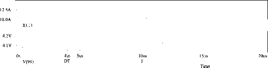 FIGURE 10.32 Waveforms of the forward converter with practical transformer and output filtering capacitor having nonzero series effective resistance. 4.0A OA -4.0A the assumption that transformer effectively has no leakage inductance (with coupling coefficient К = 0.99999999). However, it is found that when a practical transformer (having a shghtly lower K) is used, severe ringings occur. Fig. 10.32 shows some simulation results to demonstrate this phenomenon and the following assumptions are made: Dp and Dp are MBR2540 Schottky diodes and D is an MUR460 uhra fast diode; Ml is an IRF640 MOS transistor; transformer has a practical coupling coefficient of 0.996; the effective winding resistance of Lp is 0.1 Q, the effective winding resistance of Lj is 0.4 Q, and the effective winding resistance of is 0.01 Q; the effective series resistance of the output filtering capacitor is 0.05 Q; and the switching operation of the converter has reached a steady state. The resultant waveforms shown in Fig. 10.32 indicate that there are large voltage and current ringings in the circuit. These ringings are caused by the resonant circuits formed by the leakage inductance of the transformer and the parasitic capacitances of the diodes and the transistor. Therefore, a practical converter may need snubber circuits to damp these ringings, as will be described in what follows. 10.6.1.5 Circuit with Snubber Across Transformer To suppress the ringing voltage caused by the resonant circuit formed by transformer leakage inductance and the parasitic capacitance of the MOS switch, a snubber circuit, shown as Ri and Q in Fig. 10.33, is now connected across the primary winding of transformer T. The new waveforms are shown in Fig. 10.34. Fiere the drain-to-source voltage waveform of the 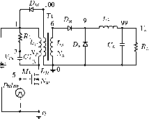 FIGURE 10.33 Forward converter with snubber circuit (RiC) across transformer: V = 50У; = MUR460; = MBR2540: Dp = MBR2540; = IRF640; = 24 Q; Q = 3000 pF; Cp = 3500 iF; ESR of Cp = 0.05 Q; = S iH; Lp = 0.576 mH Lm = 0.576 mH; Ls = О.ОЗбтН; Np : : Ns = 4 : 4 :l; Rp = 0.35 Q; effective winding resistance of = 0.1 Q; effective winding resistance of = 0.4 Q; effective winding resistance of L = 0.01 Q; and coupling coefficient k = 0.996. MOS transistor V(3) is found to be acceptable. Fiowever, there are still large ringing voltages across the output rectifiers (V(6, 9) and V(9)). To damp the ringing voltages across the output rectifiers, additional snubber circuits across the rectifiers may therefore also be required in a practical circuit, as will be described in what follows. 10.6.1.6 Practical Circuit Fig. 10.35 shows a practical forward converter also with snubber circuits added to rectifiers (i2Q Dp and RC for Dp) to reduce voltage ringing. Figs. 10.36 and 10.37 show the resultant voltage and current waveforms. Fig. 10.36 is for continuous-mode operation (ij = 0.35 Q), where I(Li) (current in Li) is continuous. Figure 10.37 is for discontinuous-mode operation {Rp = 10 Q), where I(Li) becomes discontinuous due to an increased value of Rp. These waveforms are considered to be acceptable. The design considerations of diode rectifier circuits in high-frequency converters will be discussed later in Section 10.6.3. 10.6.2 Flyback Rectifier Diode and Clamping Diode in a Flyback Converter 10.6.2.1 Ideal Circuit Fig. 10.38 shows the basic circuit of a flyback converter. Due to its simple circuit, this type of converter is widely used in low-cost low-power applications. Discontinuous-mode operation (meaning that the magnetizing current in the transformer falls to zero before the end of each switching cycle) is often used because it offers the advantages of easy control and low diode reverse-recovery loss. Fig. 10.39 shows the idealized steady-state waveforms for discontinuous-mode operation. These waveforms are obtained from PSpice simulations, based on the following assumptions: Dp is an idealized rectifier diode with infinitely fast switching speed; Ml is an idealized MOS switch with infinitely fast switching speed, with on-state resistance of 0.067 Q; and off-state resistance of 1 MQ; transformer has a coupling coefficient of 0.99999999; and the switching operation of the converter has reached a steady state. Referring to the circuit shown in Fig. 10.38 and the waveforms shown in Fig. 10.39, the operation of the converter can be explained as follows: 1. For 0 < t < DT The switch is turned on at t = 0 and V(3) = 0 for 0 < t < DT.
□ Vl(VPULSE) □ I(DM) □ ID(Ml) □ V(IOO) □ V(3) □ V(6) □ V(9) □ V(6,9)  □ I(DR) OA--20A □ I(DF) 15.0A 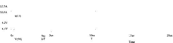 FIGURE 10.34 Waveforms of the forward converter with snubber circuit across transformer. l.OA OA -l.OA 4.0A OA -4.0A lOOV OV -lOOV 200V OV -200V 50V OV -50V 40V OV -40V 40V OV -40V 1 ... 13 14 15 16 17 18 19 ... 91 |
||||||||||||||||||||||||||||||||||||||||||||||||||||||||||||||||||||||||||||||||||||||||||||||||||||||||||||||||||||||||||||||||||||||||||||||||||
|
© 2026 AutoElektrix.ru
Частичное копирование материалов разрешено при условии активной ссылки |