 |
 |
 |
| Главная Журналы Популярное Audi - почему их так назвали? Как появилась марка Bmw? Откуда появился Lexus? Достижения и устремления Mercedes-Benz Первые модели Chevrolet Электромобиль Nissan Leaf |
Главная » Журналы » Metal oxide semiconductor 1 ... 14 15 16 17 18 19 20 ... 91
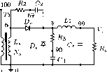 FIGURE 10.35 Practical forward converter with snubber circuits across transformer and rectifiers: V = 50 V; Dj = MUR460; Dp = MBR2540; Dp = MBR2540; = IRF640; = 24 Q; R2 = 10 Q; R = 10 Q; Q = 3000 pF; c2 = 10 nF; C3 = 10 nF; Cp = 3500 iF; ESR of Cp = 0.05 Q; Li = 8 iH; Lp = 0.576 mH; L = 0.576 mH; Ls = О.ОЗбтН; Np : : = 4 : 4 : 1; effective winding resistance of = 0.1 Q; effective winding resistance of L = 0.4 Q; and effective winding resistance of L = 0.01 Q; and coupling coefficient К = 0.996. The current in M, denoted as ID(Mi), increases at the rate of ID(Mi) у1 (10.99) The output rectifier Dp is reversely biased. 2. For DT <t < (D + D2)T The switching is turned off at t = DT. The collapse of magnetic flux induces a back emf in L5 to turn on the output rectifier Dp. The initial amplitude of the rectifier current I(DR), which is also denoted as I(LS), can be found by equating the energy stored in the primary-winding current I(LP) just before t = DT to the energy stored in the secondary-winding current I(LS) just after t = DT: Lp(I(LP))=L5(I(LS)) I(LS)= V s Lp (10.100) (10.101) (10.102) and I(LS) falls to zero at t = (D + D2)T. As D2V,= VUNs/Np)D, D2=D Vo Np (10.105) D2 is effectively the duty cycle of the output rectifier Dp. 3. For (D + D2)T <t<T The output rectifier Dp is off. The output capacitor Q provides the output current to the load Rp. The switching cycle restarts when the switch is turned on again at t = T. From the waveforms shown in Fig. 10.39, the following information (for discontinuous-mode operation) can be obtained: The maximum value of the current in the switch is ID(Mi)ax=y Lp (10.106) The maximum value of the current in the output rectifier Dp is I(DR) = T Ns Lp (10.107) The output voltage can be found by equating the input energy to the output energy within a switching cycle iN [Charge taken from V in a switching cycle (10.108) (10.109) The maximum reverse voltage of Dp, V(6, 9) (which is the voltage at node 6 with respect to node 9), is V(DR) = y(6, 9) = V,+V, (10.110) I(LS) = The amplitude of I(LS) falls at the rate of I(LS)-y, dt Lc (10.103) (10.104) 10.6.2.2 Practical Circuit When a practical transformer (with leakage inductance) is used in the flyback converter circuit shown in Fig. 10.38, there will be large ringings. In order to reduce these ringings to levels that are acceptable under actual conditions, snubber and clamping circuits have to be added. Fig. 10.40 shows a practical flyback converter circuit where a resistor-capacitor □ Vl(VPULSE) □ I(DM) OA 4 -4.0A □ ID(Ml) lOOV -lOOV □ V(IOO) 200V OV -200V 20V OV -20V 20V OV -20V 20V OV -20V □ V(3) □ V(6) □ V(9) □ V(6,9) 20A-OA--20A - □ I(DR) 20A OA -20A □ I(DF) 15.0A 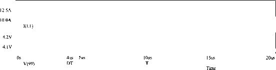 FIGURE 10.36 Waveforms of practical forward converter for continuous-mode operation. l.OA OA -l.OA 4.0A 500mA OA -500mA □ Vl(VPULSE) □ I(DM) 2.0A OA -2.0A lOOV ov-l -lOOV □ ID(Ml) □ V(IOO) 200V OV -200V □ V(3) OV -20V □ V(6) -20V □ V(9) -40V 4.0A OA -4.0A □ V(6,9) □ I(DR) 4.0A OA -4.0A 4.0A OA -4.0A □ I(DF) □ I(L1) 7.6V □ V(99) 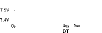 lOus T 15us Time 20us FIGURE 10.37 Waveforms of practical forward converter for discontinuous-mode operation. 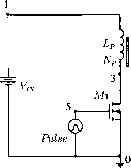
= 100 pF Lp= 100 ЛН L = 400iiH д^, = 4ооа Np:Ns=l:2 FIGURE 10.38 Basic circuit of flyback converter. snubber {R2C2) is used to damp the ringing vohage across the output rectifier Dj and a resistor-capacitor-diode clamping (RiCiDg) is used to clamp the ringing voltage across the switch Ml. The diode here allows the energy stored by the current in the leakage inductance to be converted to the form of a dc voltage across the clamping capacitor Q. The R2 C2 rwv-Ih-i Pulse FIGURE 10.40 Ds = MUR460; flyback converter circuit: = 60 V; ml = IRF640; = 4.7 KQ; Practical Dr = MUR460; R2 = 100 Q; Q = 0.1 iF; c2 = 680 pF; Q = 100 iF; ESR of Q = 0.05 Q; Lp = 100 iH; Ls = 400 iH; = 400 Q; Np : Ns = I : 2; effective winding resistance of = 0.025 Q; effective winding resistance oiLs = 0.1 Q; and coupling coefficient К = 0.992. energy transferred to Q is then dissipated slowly in the parallel resistor R without ringing problems. The simulated waveforms of the flyback converter (circuit given in Fig. 10.40) for discontinuous-mode operation are □ Vl(VPULSE) 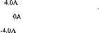 □ ID(Ml) 200V OV -200V □ V(3) 200V -200V □ V(6) 109.2V 109.1V ч 109.0V □ V(9) 400V OVH -400V □ V(6,9) 2.0A OA -2.0A Os 4us 5us □ I(DR)orI(LS) DT lOus (D+D2)T T 15us Time 20us FIGURE 10.39 Idealized steady-state waveforms of flyback converter for discontinuous-mode operation.
□ Vl(VPULSE) 4.0A OA -4.0A 200V OV -200V 200V -200V □ ID(Ml) □ V(3) □ V(6) 98.8V 98.6V 400V
□ V(9) OV--400V □ V(6,9) l.OA OA -l.OA 2.0A OA -2.0A  □ I(DR) □ I(DS) 200V -200V □ V(3,2) 4us 5us DT lOus (D+D2)T T 15us Time 20us FIGURE 10.41 Waveforms of practical flyback converter for discontinuous-mode operation. shown in Fig. 10.41, where the following assumptions are made: Dp and Ds are MUR460 uhra-fast diodes; Ml is an IRF640 MOS transistor; transformer has a practical coupling coefficient of 0.992; the effective winding resistance of Lp is 0.025 Q and the effective winding resistance of L is 0.1 Q; the effective series resistance of the output filtering capacitor Q is 0.05 Q; and the switching operation of the converter has reached a steady state. The waveforms shown in Fig. 10.41 are considered to be acceptable. 10.6.3 Design Considerations It is necessary for the designer of rectifier circuits to determine the voltage and current ratings of the diodes. The ideahzed waveforms and expressions for the maximum diode voltages and currents given in Section 10.6.2.1 (for both forward and flyback converters) are a good starting point. Fiowever, when parasitic/stray components are also considered, the simulation results given in Section 10.6.1.6 are much more useful for determination of the voltage and current ratings of high-frequency rectifier diodes. Assuming that the voltage and current ratings have been determined, diodes can be selected that meet the requirements. The following are some general guidelines on the selection of diodes: For low-voltage applications, Schottky diodes should be used because they have very fast switching speed and low forward voltage drop. If Schottky diodes cannot be used, either because of their low reverse breakdown voltage or because of their large leakage current (when reversely biased), ultra-fast diodes should be used. The reverse breakdown-voltage rating of the diode should be reasonably higher (e.g., 10% or 20% higher) than the maximum reverse voltage the diode is expected to encounter under the worst-case condition. However, an overly conservative design (using a diode with much higher breakdown voltage than necessary) would result in a lower rectifier efficiency, because a diode having a higher reverse-voltage rating would normally have a larger voltage drop when it is conducting. The current rating of the diode should be substantially higher than the maximum current the diode is expected to carry during normal operation. Using a diode with a relatively large current rating has the following advantages: (i) It reduces the possibility of damage due to transients caused by start-up, accidental short circuit, or random turning on and off of the converter. (ii) It reduces the forward voltage drop because the diode is operated in the lower current region of the V-I characteristic. In some of the high-efficiency converter circuits, the current rating of the output rectifier can be many times larger than the actual current expected in the rectifier. In this way, higher efficiency is achieved at the expense of a larger silicon area. In the design of RC snubber circuits for rectifiers, it should be understood that a larger С (and a smaller R) wiU give better damping. However, a large С (and a smaU R) will result in a large switching loss (which is equal to 0.5 CVf). As a guide-hne, a capacitor with 5 to 10 times the junction capacitance of the rectifier may be used as a starting point for iterations. The resistor chosen should be able to provide a slightly under-damped operating condition. 10.6.4 Precautions in Interpreting Simulation Results In using the simulated waveforms as references for design purposes, attention should be paid to the foUowing: The voltage/current spikes that appear in those waveforms measured under actual conditions may not appear in the simulated waveforms. This is due to the lack of a model in computer simulation that is able to simulate unwanted coupling among the practical components. Most of the computer models of diodes, including those used in the simulations given here, do not take into account the effects of forward recovery time. (The forward recovery time is not even mentioned in most manufacturers data sheets.) However, it is also interesting to note that in most cases the effect of forward recovery time of a diode is masked by that of the effective inductance in series with the diode (e.g., the leakage inductance of a transformer). References 1. Rectifier Applications Handbook, 3rd ed., Phoenix, Ariz.: Motorola, Inc., 1993. 2. M. H. Rashid, Power Electronics: Circuits, Devices, and Applications, 2nd ed., Englewood Cliffs, NJ: Prentice Hall, Inc., 1993. 3. Y.-S. Lee, Computer-Aided Analysis and Design of Switch-Mode Power Supplies, New York: Marcel Dekker, Inc., 1993. 4. J. W. Nilsson, Introduction to PSpice Manual, Electric Circuits Using OrCAD Release 9.1, 4th ed.. Upper Saddle River, NJ: Prentice Hall, Inc., 2000. 5. J. Keown, OrCAD PSice and Circuit Analysis, 4th ed.. Upper Saddle River, NJ: Prentice Hall, Inc., 2001. Single-Phase Controlled Rectifiers Jose Rodriguez, Ph.D. and Alejandro Weinstein, Ph.D. Department of Electronics, Universidad Tecnica Federico Santa Maria, Valparaiso, Chile 11.1 Line Commutated Single-Phase Controlled Rectifiers................................. 169 11.1.1 Single-Phase Half-Wave Rectifier 11.1.2 Biphase Half-Wave Rectifier 11.1.3 Single-Phase Bridge Rectifier 11.1.4 Analysis of the Input Current 11.1.5 Power Factor of the Rectifier 11.1.6 The Commutation of the Thyristors 11.1.7 Operation in the Inverting Mode 11.1.8 Applications 11.2 Unity Power Factor Single-Phase Rectifiers............................................... 175 11.2.1 The Problem of Power Factor in Single-Phase Line-Commutated Rectifiers 11.2.2 Standards for Harmonics in Single-Phase Rectifiers 11.2.3 The Single-Phase Boost Rectifier 11.2.4 Voltage Doubler PWM Rectifier 11.2.5 The PWM Rectifier in Bridge Connection 11.2.6 Applications of Unity Power Factor Rectifiers 11.2.6.1 Boost Rectifier 11.2.6.2 Voltage Doubler PWM Rectifier 11.2.6.3 PWM Rectifier in Bridge Connection Acknowledgment.................................................................................. 182 References........................................................................................... 182 11.1 Line Commutated Single-Phase Controlled Rectifiers 11.1.1 Single-Phase Half-Wave Rectifier As shown in Fig. 11.1, the single-phase half-wave rectifier uses a single thyristor to control the load voltage. The thyristor will conduct, ON state, when the voltage i; is positive and a firing current pulse Iq is apphed to the gate terminal. Delaying the firing pulse by an angle a does the control of the load voltage. The firing angle a is measured from the position where a diode would naturally conduct. In Fig. 11.1 the angle a is measured from the zero crossing point of the supply voltage v. The load in Fig. 11.1 is resistive and therefore current has the same waveform as the load voltage. The thyristor goes to the nonconducting condition, OFF state, when the load voltage and, consequently, the current try to reach a negative value. The load average voltage is given by: max sin (Dtd{(Dt) = (1 + cosa) (11.1) where У^ах is the supply peak voltage. Fience, it can be seen from Eq. (11.1) that changing the firing angle a controls both the load average voltage and the power flow. Figure 11.2a shows the rectifier waveforms for an - L load. When the thyristor is turned ON, the voltage across the inductance is l = s-r = L (11.2) The voltage in the resistance R is Vp = R - i. While Vs - Vp> 0, Eq. (11.2) shows that the load current increases its value. On the other hand, decreases its value when Vs ~ < - The load current is given by i(cot) = vpde (11.3) Graphically, Eq. (11.3) means that the load current is equal to zero when = a2, maintaining the thyristor in conduction state even when v, < 0. 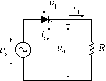
FIGURE 11.1 Single thyristor rectifier with resistive load. Area A, 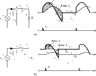 FIGURE 11.2 Single thyristor rectifier with: (a) resistive-inductive load; and (b) active load. When an inductive-active load is connected to the rectifier, as depicted in Fig. 11.2b, the thyristor will be turned ON if the firing pulse is applied to the gate when > E. Again, the thyristor wiU remain in the ON state until = A2. When the thyristor is turned OFF, the load voltage will be = E. 11.1.2 Biphase Half-Wave Rectifier The biphase half-wave rectifier shown in Fig. 11.3 uses a center-tapped transformer to provide two voltages and 12 These two voltages are 180° out-of-phase with respect to the mid-point neutral N. In this scheme, the load is fed via a thyristor in each positive cycle of voltages Vi and V2 and the load current returns via the neutral N. With reference to Fig. 11.3, thyristor can be fired into the ON state at any time provided that voltage Vji > 0. The firing pulses are delayed by an angle a with respect to the instant where diodes would conduct. Figure 11.3 also iUustrates the current paths for each conduction state. Thyristor remains in the ON state until the load current tries to go to a negative value. Thyristor T2 is fired into the ON state when Vt2 > 0? which corresponds in Fig. 11.3 to the condition at which V2 > 0. The mean value of the load voltage with resistive load is given by max sin CDtd(CDt) = Kl+cosa) (11.4) 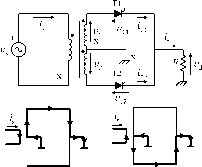 3=1-if    FIGURE 11.3 Biphase half-wave rectifier. Ш 1.0 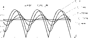 FIGURE 11.4 Effect of the load time constant over the current ripple. firing angle a = 0°. The ripple in the load current reduces as the load inductance increases. If the load inductance L 00, then the current is perfectly filtered. The ac supply current is equal to iji(N2/Ni) when is in the on-state and - 72(2/1) when T2 is in the on-state, where N2/N1 is the transformer turns ratio. Figure 11.4 shows the effect of the load time constant Ti = L/R on the normahzed load current ij(0/j?(0 for a 11.1.3 Single-Phase Bridge Rectifier Figure 11.5a shows a fully controUed bridge rectifier, which uses four thyristors to control the average load voltage. In Load V(y) h Load FIGURE 11.5 Single-phase bridge rectifier: (a) fijUy controlled; and (b) half controlled. addition, Fig. 11.5b shows the half-controlled bridge rectifier, which uses two thyristors and two diodes. Figure 11.6 shows the voltage and current waveforms of the fully controlled bridge rectifier for a resistive load. Thyristors Tl and t2 must be fired simultaneously during the positive half wave of the source voltage so as to allow conduction of current. Alternatively, thyristors T3 and T4 must be fired simultaneously during the negative half wave of the source voltage. To ensure simultaneous firing, thyristors and T2 use the same firing signal. The load voltage is similar to the voltage obtained with the biphase half-wave rectifier. The input current is given by % = hi - (11.5) and its waveform is shown in Fig. 11.6. 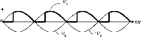
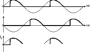 FIGURE 11.6 resistive load. Waveforms of a fully controlled bridge rectifier with Ш FIGURE 11.7 Waveforms of a fully controlled bridge rectifier with resistive-inductive load {L 00). Figure 11.7 presents the behavior of the fully controlled rectifier with resistive-inductive load (with L 00). The high-load inductance generates a perfectly filtered current and the rectifier behaves like a current source. With continuous load current, thyristors and T2 remain in the on-state beyond the positive half-wave of the source voltage v. For this reason, the load voltage can have a negative instantaneous value. The firing of thyristors T3 and T4 has two effects: i) they turn off thyristors and t2; and ii) after the commutation they conduct the load current. This is the main reason why this type of converter is called a naturally commutated or line commutated rectifier. The supply current % has the square waveform shown in Fig. 11.7 for continuous conduction. In this case, the average load voltage is given by Vs.-- V Sin cotd(cot) = COS a (11.6) 11.1.4 Analysis of the Input Current The input current in a bridge-controlled rectifier is a square waveform when the load current is perfectly filtered. In addition, the input current is shifted by the firing angle a with respect to the input voltage v, as shown in Fig. 11.8a. The input current can be expressed as a Fourier series, where the amplitude of the different harmonics is given by J.max =J ( =1,3,5,...) (11.7) where n is the harmonic order. The root mean square (rms) value of each harmonic can be expressed as cos(z)i = cos a (11.12) In the case of nonsinusoidal current, the active power delivered by the sinusoidal single-phase supply is V2 71 n (11.8) vXt)iXt)dt = cos (11.13) Thus, the rms value of the fundamental current L is 2 /2 (11.9) It can be observed from Fig. 11.8a that the displacement angle Ф1 of the fundamental current ii corresponds to the firing angle a. Fig. 11.8b shows that in the harmonic spectrum of the input current, only odd harmonics are present with decreasing amplitude. The rms value of the input current is L = L (11.10) The total harmonic distortion (THD) of the input current is given by THD = 100 = 48.4/ (11.11) where is the rms value of the single-phase voltage v. The apparent power is given by S = V± The power factor (PF) is defined by (11.14) (11.15) Substitution from Eqs. (11.12), (11.13), and (11.14) in Eq. (11.15) yields: PF = cosa (11.16) This equation shows clearly that due to the nonsinusoidal waveform of the input current, the power factor of the rectifier is negatively affected by both the firing angle a and the distortion of the input current. In effect, an increase in the 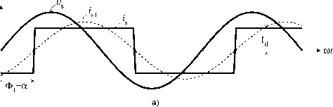 .11- FIGURE 11.8 Input current of the single-phase controlled rectifier in bridge connection: (a) waveforms; and (b) harmonics spectrum. 11.1.5 Power Factor of the Rectifier The displacement factor of the fundamental current, obtained from Fig. 11.8a, is 1 ... 14 15 16 17 18 19 20 ... 91 |
||||||||||||||||||||||||||||||||||||||||||||||||||||||||||||||||||||
|
© 2026 AutoElektrix.ru
Частичное копирование материалов разрешено при условии активной ссылки |