 |
 |
 |
| Главная Журналы Популярное Audi - почему их так назвали? Как появилась марка Bmw? Откуда появился Lexus? Достижения и устремления Mercedes-Benz Первые модели Chevrolet Электромобиль Nissan Leaf |
Главная » Журналы » Metal oxide semiconductor 1 ... 15 16 17 18 19 20 21 ... 91 distortion of the current produces an increase in the value of in Eq. (11.16), which deteriorates the power factor. 11.1.6 The Commutation of the Thyristors Until now the current commutation between thyristors has been considered to be instantaneous. This consideration is not vahd in real cases due to the presence of the line inductance L, as shown in Fig. 11.9a. During commutation, the current through the thyristors cannot change instantaneously, and for this reason, during the commutation angle ju, all four thyristors are conducting simultaneously. Therefore, during the commutation the following relationship for the load voltage holds: = 0 ot < cot < ot -\- fi (11.17) The effect of the commutation on the supply current, voltage waveforms, and the thyristor current waveforms is observed in Fig. 11.9b. 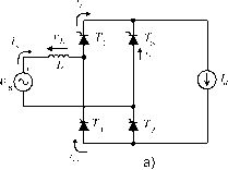 During commutation the following expression holds: L = i; =y sincot а<М<а-\-1л (11.18) at Integrating Eq. (11.18) over the commutation interval yields h у ] max dts=-r--h sin cotdt (11.19) (X/(D From Eq. (11.19), the following relationship for the commutation angle jii is obtained: cos(a + ) = cos a - -(11.20) Equation (11.20) shows that an increase of the line inductance L or an increase of the load current increases the commutation angle /Л. In addition, the commutation angle is affected by the firing angle a. In effect, Eq. (11.18) shows that with different values of a, the supply voltage has a different instantaneous value, which produces different diJdt, thereby affecting the duration of the commutation. Equation (11.17) and the waveform of Fig. 11.9b show that the commutation process reduces the average load voltage V. When commutation is considered, the expression for the average load voltage is given by У Vjnax sin (Dtd{(Dt) = [cos(a + ) + COS a] (11.21) Substituting Eq. (11.20) into Eq. (11.21) yields 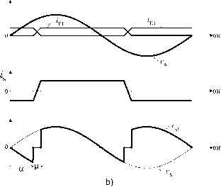 FIGURE 11.9 forms. The commutation process: (a) circuit; and (b) wave- у da =-maxCOSa--1 71 71 (11.22) II.1.7 Operation in the Inverting Mode When the angle a > 90°, it is possible to obtain a negative average load voltage. In this condition, the power is fed back to the single-phase supply from the load. This operating mode is called inverter or inverting mode, because the energy is transferred from the dc to the ac side. In practical cases this operating mode is obtained when the load configuration is as shown in Fig. 11.10a. It must be noticed that this rectifier allows unidirectional load current flow. Figure 11.10b shows the waveform of the load voltage with the rectifier in the inverting mode, neglecting the source inductance L. Section 11.1.6 described how supply inductance increases the conduction interval of the thyristors by the angle ju. As 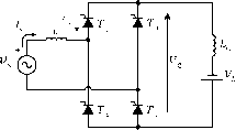 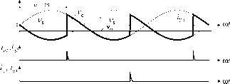    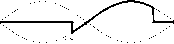 FIGURE 11.10 Rectifier in the inverting mode: (a) circuit; (b) waveforms neglecting source inductance L; and (c) waveforms considering L. shown in Fig. 11.10c, the thyristor voltage Vji has a negative value during the extinction angle 7, defined by у = 180 - (a+ ) (11.23) To ensure that the outgoing thyristor wiU recover its blocking capability after commutation, the extinction angle should satisfy the following restriction: У > cot. (11.24) where со is the supply frequency and t is the thyristor turn-off time. Considering Eqs. (11.23) and (11.24) the maximum firing angle is, in practice. = 180--7 (11.25) If the condition of Eq. (11.25) is not satisfied, the commutation process will fail and then destructive currents will occur. Grid Load FIGURE 11.11 Application of a rectifier in single-phase UPS. 11.1.8 Applications Important application areas of controUed rectifiers include uninterruptible power supplies (UPS) for feeding critical loads. Figure 11.11 shows a simplified diagram of a single-phase UPS configuration, typically rated for < lOkVA. A fully controUed or half-controUed rectifier is used to generate the dc voltage for the inverter. In addition, the input rectifier acts as a battery charger. The output of the inverter is filtered before it is fed to the load. The most important operational modes of the UPS are: i) Normal mode. In this case the hne voltage is present. The critical load is fed through the rectifier-inverter scheme. The rectifier keeps the battery charged. Outage mode. During a loss of the ac main supply, the battery provides the energy for the inverter. Bypass operation. When the load demands an over-current to the inverter, the static bypass switch is turned on and the critical load is fed directly from the mains. ii) iii) The control of low-power dc motors is another interesting application of controUed single-phase rectifiers. In the circuit of Fig. 11.12, the controlled rectifier regulates the armature voltage and consequently controls the motor current in order to establish a required torque. This configuration aUows only positive current flow in the load. However, the load voltage can be both positive and negative. For this reason, this converter works in the two-quadrant mode of operation in the plane vs V. 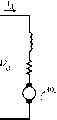 a) b) FIGURE 11.12 Two quadrant dc drive: (a) circuit; and (b) quadrants of operation. 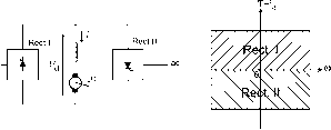 FIGURE 11.13 Single-phase dual-converter drive: (a) connection; and (b) four-quadrant operation. As shown in Fig. 11.13, a better performance can be obtained with two rectifiers in back-to-back connection at the dc terminals. This arrangement, known as a dual converter one, allows four-quadrant operation of the drive. Rectifier I provides positive load current ij, while rectifier II provides negative load current. The motor can work in forward powering, forward braking (regenerating), reverse powering, and reverse braking (regenerating). These operating modes are shown in Fig. 11.13b, where the torque T vs the rotor speed CDp is illustrated. 11.2 Unity Power Factor Single-Phase Rectifiers 11.2.1 The Problem of Power Factor in Single-Phase Line-Commutated Rectifiers The main disadvantages of classical fine-commutated rectifiers are that i) they generate both a lagging displacement factor with respect to the voltage of the utility, and ii) an important amount of input current harmonics. These aspects have a negative influence on both power factor and power quality. In the last several years, the massive use of single-phase power converters has increased the problems of power quality in electrical systems. In effect, modern commercial buildings have 50% and even up to 90% of the demand originated by nonhnear loads, which are composed mainly of rectifiers [1]. Today it is not unusual to find rectifiers with total harmonic distortion of the current TFiD > 40% originating severe overloads in conductors and transformers. Figure 11.14 shows a single-phase rectifier with a capacitive filter, used in much of todays low power equipment. The input current is highly distorted due to the presence of the filter capacitor. This current has a harmonic content as shown in Fig. 11.15 and Table 11.1, with a THD = 197%. The rectifier of Fig. 11.14 has a very low power factor of PF = 0.45, due mainly to its large harmonic content. 11.2.2 Standards for Harmonics in Single-Phase Rectifiers The relevance of the problems originated by harmonics in line-commutated single-phase rectifiers has motivated some agencies to introduce restrictions to these converters. The lEC 1000-3-2 International Standard establishes limits to all low-power single-phase equipment having an input current with a special wave shape and an active input power P < 600 W. Class D equipment has an input current with a special wave shape contained within the envelope given in Fig. 11.14b. This class of equipment must satisfy certain harmonic hmits, shown in Fig. 11.15. It is clear that a single-phase line-commutated rectifier with parameters as shown in Fig. 11.14a is not able to comply with the standard lEC 1000-3-2 Class D. The standard can be satisfied only by adding huge passive filters, which increases the size, weight, and cost of the s L Lr>r>r> 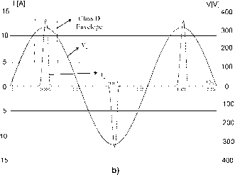 FIGURE 11.14 Single-phase rectifier: (a) circuit; and (b) waveforms of the input voltage and current. 2000 - 1500 - 1000 500 - Amplitude mA □ Standard lEC 1000 3 2 Class D l-t I.I ill I ! I- f- > 1 2 3 4 5 6 7 8 9 10 11 12 13 14 15 16 17 18 19 20 21 22 23 24 25 26 27 28 29 30 31 32 33 34 35 36 37 38 39 40 FIGURE 11.15 Harmonics in the input current of the rectifier of Fig. 11.14. TABLE 11.1 Harmonics in percentage of the current in Fig. 11.14
through the transistor. The current of the inductance ii is given by the foUowing equation dtLVL dt L (11.26) rectifier. This standard has been the motivation for the development of active methods to improve the quality of the input current and, consequently, the power factor. 11.2.3 The Single-Phase Boost Rectifier From both the theoretical and conceptual points of view, one of the most important high-power factor rectifiers is the so-called single-phase boost rectifier, shown in Fig. 11.16a. This rectifier is obtained from a classical noncontroUed bridge rectifier, with the addition of transistor T, diode D, and inductor L In this rectifier, the input current i(t) is controUed by changing the conduction state of transistor T. When transistor T is in the ON state, the single-phase power supply is short-circuited through the inductance L, as shown in Fig. 11.16b; the diode D avoids the discharge of the filter capacitor С Due to the fact that > 0, the ON state of transistor T always produces an increase in the inductance current ii and.
FIGURE 11.16 Single-phase boost rectifier: (a) power circuit and equivalent circuit for transistor T in (b) ON-state and (c) OFF-state. 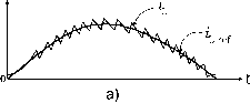 FIGURE 11.17 Behavior of the inductor current z: (a) waveforms; and (b) transistor T gate drive signal x. consequently, an increase in the absolute value of the source current i. When transistor T is turned OFF, the inductor current ip cannot be interrupted abruptly and flows through diode D, charging capacitor C. This is observed in the equivalent circuit of Fig. 11.16c. In this condition the behavior of the inductor current is described by (11.27) If > which is an important condition for the correct behavior of the rectifier, then - < 0, and this means that in the OFF state the inductor current decreases its instantaneous value. With an appropriate firing pulse sequence applied to transistor T, the waveform of the input current i can be controlled to follow a sinusoidal reference, as can be observed in the positive halfwave of i in Fig. 11.17. This figure shows the reference inductor current ijef the inductor current ip, and the gate drive signal x for transistor T. Transistor T is ON when X = 1 and it is OFF when x = 0 . Figure 11.17 clearly shows that the ON(OFF) state of transistor T produces an increase (decrease) in the inductor current ip. Figure 11.18 presents a block diagram of the control system for the boost rectifier, which includes a proportional-integral (PI) controller to regulate the output voltage V. The reference value ijj.gf for the inner current control loop is obtained from 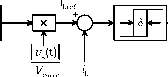 FIGURE 11.18 Control system of the boost rectifier. the multiplication between the output of the voltage controller and the absolute value i;t). A hysteresis controller provides a fast control for the inductor current ip, resulting in a practically sinusoidal input current i. Typically, the output voltage should be at least 10% higher than the peak value of the source voltage v(t) in order to assure good dynamic control of the current. The control works with the following strategy: a step increase in the reference voltage Vj.gf will produce an increase in the voltage error Vj.gf - and an increase of the output of the PI controller, which originates an increase in the amplitude of the reference current ii. The current controller will follow this new reference and increase the amplitude of the sinusoidal input current i, which will increase the active power delivered by the single-phase supply and finally produce an increase in the output voltage V. Figure 11.19a shows the waveform of the input current i and the source voltage v. The ripple of the input current can be diminished by reducing the hysteresis width S. The price to be paid for this improvement is an increase in switching frequency, which is proportional to the commutation losses of transistor T. For a given hysteresis width d, a reduction of inductance L also produces an increase in the switching frequency. A drastic reduction in the harmonic content of input current i can be observed in the frequency spectrum of Fig. 11.19b. This current complies with the restrictions established by lEC standard 1000-3-2. The total harmonic distortion of the current in Fig. 11.19a is TFiD = 4.96% and the power factor of the rectifier is PF = 0.99. Figure 11.20 shows the dc voltage control loop dynamic behavior for step changes in the load. An increase in the load, at t = 0.3 [s], produces an initial reduction of the output voltage V, which is compensated by an increase in the input current i. At t = 0.6 [s] a step decrease in the load is applied. The dc voltage controller again adjusts the supply current in order to balance the active power. 11.2.4 Voltage Doubler PWM Rectifier Figure 11.21a shows the power circuit of the voltage doubler pulsewidth modulated (PWM) rectifier, which uses two transistors and two filter capacitors and c2. Transistors and t2 are switched in complement to control the waveform of input current i and output dc voltage V. Capacitor voltages Vqi and must be higher than the peak value of the input voltage to ensure control of the input current. The equivalent circuit of this rectifier with transistor in the ON state is shown in Fig. 11.21b. The inductor voltage dynamic equation is = J = 5(0 -Vci<0 (11.28) 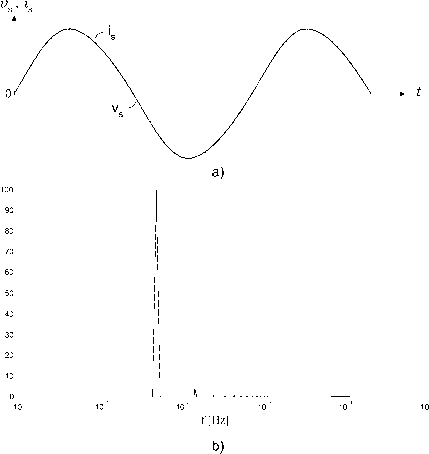 FIGURE 11.19 Input current of the single-phase boost rectifier: (a) voltage and current waveforms; and (b) frequency spectrum. Vo[V] 0.2 0.3 0.4 0.5 0.6 0.7 0.8 Load rp b) b) c) FIGURE 11.20 Response to a change in the load: (a) output-voltage V; FIGURE 11.21 Voltage doubler rectifier: (a) power circuit; (b) equiva-and (b) input current z. lent circuit with ON; and (c) equivalent circuit with T2 ON. 11 Single-Phase Controlled Rectifiers PI Oref FIGURE 11.22 Control system of the voltage doubler rectifier. In this topology, the output voltage must be higher than the peak value of the ac source voltage in order to ensure proper control of the input current. Figure 11.24b shows the equivalent circuit with transistors Tl and T4 ON. In this condition, the inductor voltage is given by Equation (11.28) means that under this conduction state, current i(t) decreases its value. On the other hand, the equivalent circuit of Fig. 11.21c is vahd when transistor T2 is in the conduction state, resulting in the following expression for the inductor voltage VL = L = Vs(t)Vc2>0 (11.29) hence, for this condition the input current i(t) increases. Therefore, the waveform of the input current can be controlled by appropriately switching transistors and T2 in a similar way as shown in Fig. 11.17a for the single-phase boost converter. Figure 11.22 shows a block diagram of the control system for the voltage doubler rectifier, which is very similar to the control scheme of the boost rectifier. This topology can present an unbalance in the capacitor voltages Vqi and Vc2 which will affect the quality of the control. This problem is solved by adding to the actual current value an offset signal proportional to the capacitor voltages difference. Figure 11.23 shows the waveform of the input current. The ripple amplitude of this current can be reduced by decreasing the hysteresis of the controller. 11.2.5 The PWM Rectifier in Bridge Connection Figure 11.24a shows the power circuit of the fully controlled single-phase PWM rectifier in bridge connection, which uses four transistors with antiparallel diodes to produce a controlled dc voltage V. Using a bipolar PWM switching strategy, this converter may have two conduction states: i) transistors and T4 in the ON state and T2 and T3 in the OFF state; or ii) transistors T2 and T3 in the ON state and and T4 in the OFF state. VL = L = v,(t)-Vo<0 (11.30) 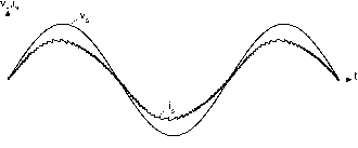 Therefore, in this condition a decrease in the inductor current 4 is produced. Figure 11.24c shows the equivalent circuit with transistors T2 and T3 ON. Fiere, the inductor voltage has the following expression VL = L = v,(t)V,>0 (11.31) which means an increase in the instantaneous value of the input current 4. 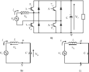 Load 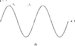 FIGURE 11.23 Waveform of the input current in the voltage doubler rectifier. FIGURE 11.24 Single-phase PWM rectifier in bridge connection: (a) circuit; (b) equivalent circuit with and Г4 ON; (c) equivalent circuit with T2 and г3 ON; and (d) waveform of the input current during regeneration. The waveform of the input current can be controUed by appropriately switching transistors t1-T4 or t2-T3, creating a shape similar to the one shown in Fig. 11.17a for the single-phase boost rectifier. The control strategy for the rectifier is similar to the one depicted in Fig. 11.22 for the voltage doubler topology. The quality of the input current obtained with this rectifier is the same as that presented in Fig. 11.23 for the voltage doubler configuration. Finally, it must be said that one of the most attractive characteristics of the fully controUed PWM converter in bridge connection and the voltage doubler is their regeneration capability. In effect, these rectifiers can deliver power from the load to the single-phase supply, operating with sinusoidal current and a high power factor of PF > 0.99. Figure 11.24d shows that during regeneration the input current is 180° out-of-phase with respect to the supply voltage v, which means operation with power factor PF - 1 (PF is near to 1 because of the smaU harmonic content in the input current). 11.2.6 Applications of Unity Power Factor Rectifiers 11.2.6.1 Boost Rectifier The single-phase boost rectifier has become the most popular topology for power factor correction (PFC) in general purpose power supplies. To reduce costs, the complete control system shown in Fig. 11.18 and the gate drive circuit of the power transistor have been included in a single integrated circuit (1С), such as the UC3854 [2] or MC33262, shown in Fig. 11.25. Today there is increased interest in developing high-frequency electronic baUasts to replace the classical electromagnetic baUast in fluorescent lamps. These electronic baUasts require an ac-dc converter. To satisfy the harmonic current injection from electronic equipment and to maintain high power quality, a high-power factor rectifier can be used, as shown in Fig. 11.26 [3]. AC LINE  I I I I I I CURRENT WAVEFORM I L SJJ INPUT I MC33262 LOAD VOLTAGE SENSE FIGURE 11.25 Simplified circuit of a power factor corrector with control integrated circuit. Line-  Dimming Control Output Stage Lamp FIGURE 11.26 Functional block diagram of electronic ballast with power factor correction. 11.2.6.2 Voltage Doubler PWM Rectifier The development of low-cost compact motor drive systems is a very relevant topic, particularly in the low-power range. Figure 11.27 shows a low-cost converter for low-power induction motor drives. In this configuration a three-phase induction motor is fed through the converter from a single-phase power supply. Transistors T, t2 and capacitors Q, c2 constitute the voltage-doubler single-phase rectifier, which controls the dc link voltage and generates sinusoidal input current, working with a close-to-unity power factor [4]. On the other hand, transistors T3, T4, T5, and and capacitors Q and c2 constitute the power circuit of an asymmetric inverter that supplies the motor. An important characteristic of the power circuit shown in Fig. 11.27 is the capability of regenerating power to the single-phase mains. 11.2.6.3 PWM Rectifier in Bridge Connection Distortion of input current in the line commutated rectifiers with capacitive filtering is particularly critical in uninterruptible power supplies (UPS) fed from motor-generator sets. In effect, due to the higher value of the generator impedance, the current distortion can originate an unacceptable distortion on the ac voltage, which affects the behavior of the whole system. For this reason, it is very attractive in this application to use rectifiers with low distortion in the input current. Figure 11.28 shows the power circuit of a single-phase UPS, which has a PWM rectifier in bridge connection at the input side. This rectifier generates a sinusoidal input current and controls the charge of the battery [5]. MAINS 3 П 5 1  FIGURE 11.27 Low-cost induction motor drive. Converter Inverter THY SW  Input 1ф100У 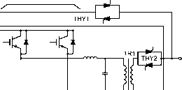 Output 1ф100V FIGURE 11.28 Single-phase UPS with PWM rectifier.  Line + transformer 4 quadrant converter DC Link Inverter FIGURE 11.29 Typical power circuit of an ac drive for a locomotive. IVIotor Perhaps the most typical and widely accepted area of apphcation of high-power factor single-phase rectifiers is in locomotive drives [6]. In effect, an essential prerequisite for proper operation of voltage source three-phase inverter drives in modern locomotives is the use of four quadrant line-side converters, which ensures motoring and braking of the drive, with reduced harmonics in the input current. Figure 11.29 shows a simplified power circuit of a typical drive for a locomotive connected to a single-phase power supply [6], which includes a high-power factor rectifier at the input. Finally, Fig. 11.30 shows the main circuit diagram of the 300 series Shinkansen train [7]. In this application, ac power from the overhead catenary is transmitted through a transformer to single-phase PWM rectifiers, which provide dc voltage for the inverters. The rectifiers are capable of controlling the input ac current in an approximate sine waveform and in phase with the voltage, achieving a power factor of close to unity for both powering and regenerative braking. Regenerative braking produces energy savings and an important operational flexibility. CONVERTER SMOOTHING CAPACITOR PWM INVERTER GTO THYRISTOR INDUCTION MOTORS FIGURE 11.30 tives. Main circuit diagram of 300 series Shinkansen locomo- Acknowledgment The authors gratefully acknowledge the valuable contribution of Dr. Ruben Peiia. References 1. R. Dwyer and D. Mueller, Selection of transformers for commercial building, Proc. IEEE/IAS 1992 Annual Meeting U.S.A., Oct. 1992, pages 1335-1342. 2. P. Todd, UC3854 controlled power factor correction circuit design, Application Note 17-134, Unitrode Corp. 3. J. Adams, T. Ribarich, and J. Ribarich, A new control 1С for dimmable high-frequency electronic ballast, IEEE Applied Power Electronics Conference APEC99, USA, 1999, pp. 713-719. 4. С Jacobina, M. Beltrao, E. Cabral, and A. Nogueira, Induction motor drive system for low-power applications, IEEE Trans. Industry Applications 35:1, 52-60 (1999). 5. K. Hirachi, H. Yamamoto, T. Matsui, S. Watanabe, and M. Nakaoka, Cost-effective practical developments of high-performance 1 kVA UPS with new system configurations and their specific control implementations, European Conference on Power Electronics EPE 95, Spain 1995, pp. 2035-2040. 6. K. Hiickelheim and Ch. Mangold, Novel 4-quadrant converter control method, European Conference on Power Electronics EPE 89, Germany 1989, pp. 573-576. 7. T. Ohmae and K. Nakamura, Hitachis role in the area of power electronics for transportation, Proceedings of the lECON 93, Hawaii, Nov. 1993, pp. 714-771. 1 ... 15 16 17 18 19 20 21 ... 91 |
||||||||||||||||||||||||||||||||||||
|
© 2026 AutoElektrix.ru
Частичное копирование материалов разрешено при условии активной ссылки |