 |
 |
 |
| Главная Журналы Популярное Audi - почему их так назвали? Как появилась марка Bmw? Откуда появился Lexus? Достижения и устремления Mercedes-Benz Первые модели Chevrolet Электромобиль Nissan Leaf |
Главная » Журналы » Metal oxide semiconductor 1 ... 17 18 19 20 21 22 23 ... 91  ТКАКЗРОЬШЕК WOUND ROTOR INDUCTION MOTOR FIGURE 12.28 Supersynchronous cascade for a wound rotor induction motor. 12.2.11 Applications in HVDC Power Transmission Fiigh voltage direct current (FiVDC) power transmission is the most powerful apphcation for hne-commutated converters that exist today. There are power converters with ratings in excess of 1000 MW. Series operation of hundreds of valves can be found in some FiVDC systems. In high-power and long distance applications, these systems become more economical than conventional ac systems. They also have some other advantages compared with ac systems: 1. they can link two ac systems operating unsynchronized or with different nominal frequencies, that is 50 Hz 60 Hz; 2. they can help in stability problems related with subsyn-chronous resonance in long ac hnes; 3. they have very good dynamic behavior, and can interrupt short-circuits problems very quickly; 4. if transmission is by submarine or underground cable, it is not practical to consider ac cable systems exceeding 50 km, but dc cable transmission systems are in service whose length is in hundreds of kilometers and even distances of 600 km or greater have been considered feasible; 5. reversal of power can be controlled electronically by means of the delay firing angles a; 6. some existing overhead ac transmission lines cannot be increased. If overbuilt with or upgraded to dc transmission this can substantially increase the power transfer capability on the existing right-of-way. The use of HVDC systems for interconnections of asynchronous systems is an interesting application. Some continental electric power systems consist of asynchronous networks such as those for the East-West Texas and Quebec networks in North America, and island loads such as that for the Island of Gotland in the Baltic Sea make good use of HVDC interconnections. Nearly all HVDC power converters with thyristor valves are assembled in a converter bridge of 12-pulse configuration, as shown in Fig. 12.29. Consequently, the ac voltages applied to each 6-pulse valve group that makes up the 12-pulse valve group have a phase difference of 30° which is utihzed to cancel POWER SYSTEM 1 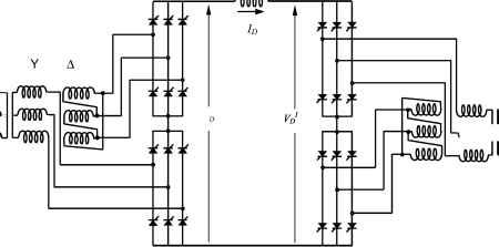 POWER SYSTEM 2  Simplified Unilinear Diagram:
Vf-f
FIGURE 12.29 Typical HVDC power system, (a) Detailed circuit; and (b) unilinear diagram. the ac side 5th and 7th harmonic currents and dc side 6th harmonic voltage, thus resulting in significant savings in harmonic filters. Some usefiil relations for HVDC systems include: (a) rectifier side: IZ(p Ip = I cos <p Iq = I sin (p An coLc [cos 2a - cos 2(a + /г)] In = cos a + cos(a + ) Fundamental secondary component of I: (12.40) (12.41) (12.42) (12.43) а^УЗ-УГГ - [sin 2(a + /г) - sin 2a - 2/г] (12.44) 4?! COLc (12.45) (12.46) 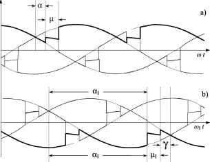 FIGURE 12.30 Definition of angle у for inverter side: (a) rectifier side; and (b) inverter side. Substituting (Eq. 12.46) into (12.45): cos a + cos(a + fi) h = I- as Ip = / cos it yields cos (p = cos a + cos(a + fi) (12.47) (12.48) (h) inverter side: The same equations are applied for the inverter side, but the firing angle a is replaced by 7, where у is (see Fig. 12.30): 7 = 180°-(a,+ ,) (12.49) As reactive power always goes in the converter direction, at the inverter side Eq. (12.44) becomes: In. =- An cOjLj [sin 2(7 + fij) - sin 27 - 2fij] (12.50) 12.2.12 Dual Converters In many variable-speed drives, four-quadrant operation is required, and three-phase dual converters are extensively used in applications up to the 2MW level. Figure 12.31 shows a three-phase dual converter, where two converters are connected back-to-back. In the dual converter, one rectifier provides the positive current to the load, and the other the negative current. Due to the instantaneous voltage differences between the output voltages of the converters, a circulating current flows through the bridges. The circulating current is normally hmited by circulating reactor Lj as shown in Fig. 12.31. The two converters are controUed in such a way that if a+ is the delay angle of the positive current converter, the delay angle of the negative current converter is a~ = 180° - a+. Figure 12.32 shows the instantaneous dc voltages of each converter, and v. Despite the average voltage Vj is the same in both the converters, their instantaneous voltage x-vVc JC  FIGURE 12.31 Dual converter in a four-quadrant dc drive. firing angle: a  lining angle: a = 180 - a 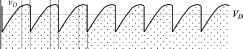 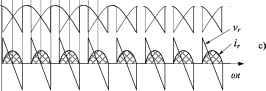 FIGURE 12.32 Waveform of circulating current: (a) instantaneous dc voltage from positive converter; (b) instantaneous dc voltage from negative converter; (c) voltage difference between and v, v, and circulating current z. differences, given by voltage v, are not producing the circulating current i, which is superimposed with the load currents i+, and i5. To avoid the circulating current i, it is possible to implement a circulating current free converter if a dead time of a few milliseconds is acceptable. The converter section not required to supply current remains fully blocked. When a current reversal is required, a logic switch-over system determines at first the instant at which the conducting converters current becomes zero. This converter section is then blocked and the further supply of gating pulses to it prevented. After a short safety interval (dead time), the gating pulses for the other converter section are released. 12.2.13 Cycloconverters A different principle of frequency conversion is derived from the fact that a dual converter is able to supply an ac load with a lower frequency than the system frequency. If the control signal of the dual converter is a function of time, the output voltage will follow this signal. If this control signal value alters sinusoidally with the desired frequency, then the waveform depicted in Fig. 12.33a consists of a single-phase voltage with a large harmonic current. As shown in Fig. 12.33b, if the load is inductive, the current will present less distortion than voltage. The cycloconverter operates in all four quadrants during a period. A pause (dead time) at least as small as the time required by the switch-over logic occurs after the current reaches zero, that is, between the transfer to operation in the quadrant corresponding to the other direction of current flow. Three single-phase cycloconverters may be combined to build a three-phase cycloconverter. The three-phase cycloconverters find an application in low-frequency, high-power 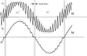 FIGURE 12.33 Cycloconverter operation: (a) voltage waveform; and (b) current waveform for inductive load. requirements. Control speed of large synchronous motors in the low-speed range is one of the most common applications of three-phase cycloconverters. Figure 12.34 is a diagram of this apphcation. They are also used to control shp frequency in wound rotor induction machines, for supersynchronous cascade (Scherbius system). 12.2.14 Harmonic Standards and Recommended Practices In view of the proliferation of power converter equipment connected to the utility system, various national and international agencies have been considering limits on harmonic  POWER TRANSFOmERS 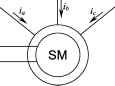 FIGURE 12.34 Synchronous machine drive with a cycloconverter. TABLE 12.1 Harmonic current limits in percent of fundamental
current injection to maintain good power quality. As a consequence, various standards and guidelines have been established that specify limits on the magnitudes of harmonic currents and harmonic voltages. The Comite Europeen de Normalisation Electrotechnique (CENELEC), International Electrical Commission (lEC), and West German Standards (VDE) specify the limits on the voltages (as a percentage of the nominal voltage) at various harmonics frequencies of the utility frequency, when the equipment-generated harmonic currents are injected into a network whose impedances are specified. In accordance with IEEE-519 standards (Institute of Electrical and Electronic Engineers), Table 12.1 lists the limits on the harmonic currents that a user of power electronics equipment and other nonlinear loads is aUowed to inject into the utility system. Table 12.2 lists the quality of voltage that the utility can furnish the user. In Table 12.1, the values are given at the point of connection of nonlinear loads. The THD is the total harmonic distortion given by Eq. (12.51), and h is the number of the harmonic. TABLE 12.2 Harmonic voltage limits in percent of fundamental THD = 
(12.51) which is not possible with line-commutated rectifiers, where thyristors are switched ON and OFF only once a cycle. This feature confers the foUowing advantages: (a) the current or voltage can be modulated (pulse width modulation or PWM), generating less harmonic contamination; (b) the power factor can be controlled, and it can even be made to lead; (c) rectifiers can be built as voltage or current source types; and (d) the reversal of power in thyristor rectifiers is by reversal of voltage at the dc link. By contrast, force-commutated rectifiers can be implemented for either reversal of voltage or reversal of current. There are two ways to implement force-commutated three-phase rectifiers: (a) as a current source rectifier, where power reversal is by dc voltage reversal; and (b) as a voltage source rectifier, where power reversal is by current reversal at the dc link. Figure 12.35 shows the basic circuits for these two topologies. The total current harmonic distortion aUowed in Table 12.1 increases with the value of short-circuit current. The total harmonic distortion in the voltage can be calculated in a manner simUar to that given by Eq. (12.51). Table 12.2 specifies the individual harmonics and the THD limits on the voltage that the utUity supplies to the user at the connection point. 12.3 Force-Commutated Three-Phase Controlled Rectifiers 12.3.1 Basic Topologies and Characteristics Force-commutated rectifiers are built with semiconductors with gate-turn-off capabUity. The gate-turn-off capability aUows fuU control of the converter, because valves can be switched ON and OFF whenever required. This aUows commutation of the valves hundreds of times in one period.  nr П dc a) load :pwm: signals: 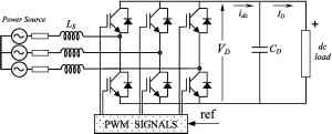 FIGURE 12.35 Basic topologies for force-commutated PWM rectifiers: (a) current source rectifier; and (b) voltage source rectifier. 12.3.2 Operation of the Voltage Source Rectifier The voltage source rectifier is by far the most widely used, and because of the duality of the two topologies showed in Fig. 12.35, only this type of force-commutated rectifier will be explained in detail. The voltage source rectifier operates by keeping the dc link voltage at a desired reference value, using a feedback control loop as shown in Fig. 12.36. To accomplish this task, the dc link voltage is measured and compared with a reference Vref-The error signal generated from this comparison is used to switch the six valves of the rectifier ON and OFF. In this way, power can come or return to the ac source according to dc link voltage requirements. Voltage is measured at capacitor C,. When the current Ip, is positive (rectifier operation), the capacitor Cp, is discharged, and the error signal ask the Control Block for more power from the ac supply. The Control Block takes the power from the supply by generating the appropriate PWM signals for the six valves. In this way, more current flows from the ac to the dc side, and the capacitor voltage is recovered. Inversely, when Ip, becomes negative (inverter operation), the capacitor Cp, is overcharged, and the error signal asks the control to discharge the capacitor and return power to the ac mains. The PWM control not only can manage the active power, but also reactive power, allowing this type of rectifier to correct power factor. In addition, the ac current waveforms can be maintained as almost sinusoidal, which reduces harmonic contamination to the mains supply. Pulsewidth-modulation consists of switching the valves ON and OFF, following a pre-established template. This template could be a sinusoidal waveform of voltage or current. For example, the modulation of one phase could be as the one shown in Fig. 12.37. This PWM pattern is a periodical waveform whose fundamental is a voltage with the same frequency of the template. The amplitude of this fundamental, called Vmod in Fig. 12.37, is also proportional to the amplitude of the template. To make the rectifier work properly, the PWM pattern must generate a fundamental Vjqd ith the same frequency as the power source. Changing the amplitude of this fundamental. 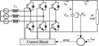     FIGURE 12.37 A PWM pattern and its fundamental Fmqd- and its phase-shift with respect to the mains, the rectifier can be controlled to operate in the four quadrants: leading power factor rectifier, lagging power factor rectifier, leading power factor inverter, and lagging power factor inverter. Changing the pattern of modulation, as shown in Fig. 12.38, modifies the magnitude of Vmod- Displacing the PWM pattern changes the phase-shift. The interaction between Vjqd (source voltage) can be seen through a phasor diagram. This interaction permits understanding of the four-quadrant capability of this rectifier. In Fig. 12.39, the following operations are displayed: (a) rectifier at unity power factor; (b) inverter at unity power factor; (c) capacitor (zero power factor); and (d) inductor (zero power factor). In Fig. 12.39 /5 is the rms value of the source current i. This current flows through the semiconductors in the same way as shown in Fig. 12.40. During the positive half cycle, the transistor T connected at the negative side of the dc hnk is switched ON, and the current begins to flow through T (Tn)- The current returns to the mains and comes back to the valves, closing a loop with another phase, and passing through a diode connected at the same negative terminal of the dc link. The current can also go to the dc load (inversion) and return through another transistor located at the positive terminal of the dc link. When the transistor T is switched OFF, the current path is interrupted, and the current begins to flow through diode Dp, connected at the positive terminal of the dc link. This current, called ij)p in Fig. 12.39, goes directly 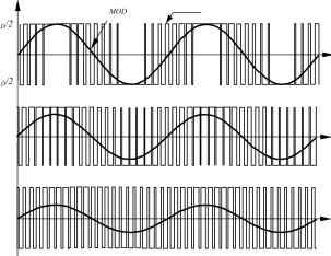 FIGURE 12.36 Operation principle of the voltage source rectifier. FIGURE 12.38 Changing Fmqd through the PWM pattern. 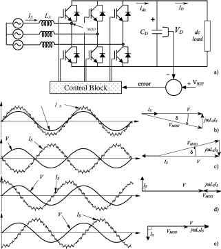 FIGURE 12.39 Four-quadrant operation of the force-commutated rectifier: (a) the PWM force-commutated rectifier; (b) rectifier operation at unity power factor; (c) inverter operation at unity power factor; (d) capacitor operation at zero power factor; and (e) inductor operation at zero power factor. to the dc link, helping in the generation of the current i. The current charges the capacitor Q and permits the rectifier to produce dc power. The inductances are very important in this process, because they generate an induced voltage that aUows conduction of the diode Dp. A similar operation occurs during the negative half cycle, but with Tp and D (see Fig. 12.40). Under inverter operation, the current paths are different because the currents flowing through the transistors come mainly from the dc capacitor Cj. Under rectifier operation, the circuit works like a Boost converter, and under inverter operation it works as a Buck converter. To have fuU control of the operation of the rectifier, their six diodes must be polarized negatively at aU values of instantaneous ac voltage supply. Otherwise, the diodes will conduct, and the PWM rectifier wiU behave like a common diode rectifier bridge. The way to keep the diodes blocked is to ensure a dc link voltage higher than the peak dc voltage generated by the diodes alone, as shown in Fig. 12.41. In this way, the diodes remain polarized negatively, and they will conduct only when at least one transistor is switched ON, and favorable instantaneous ac voltage conditions are given. In Fig. 12.41 represents the capacitor dc voltage, which is kept higher than the normal diode-bridge rectification value
 - Cd dc load FIGURE 12.40 Current waveforms through the mains, the valves, and the dc link. BRIDGE- To maintain this condition, the rectifier must have a control loop like the one displayed in Fig. 12.36. 12.3.3 PWM Phase-to-Phase and Phase-to-Neutral Voltages The PWM waveforms shown in the preceding figures are voltages measured between the middle point of the dc voltage and the corresponding phase. The phase-to-phase PWM voltages can be obtained with the help of Eq. 12.52, where the voltage У^щм is evaluated. \rAB Tm (12.52) where Vvm wm the voltages measured between the middle point of the dc voltage, and the phases a and dc link voltage Vd must remain higher than the diode rectification voltage Vbridge (feedback control loop required). Vbridge FIGURE 12.41 Direct current link voltage condition for operation of the PWM rectifier. 200. 100. 0. -100. -200. -300. 600. 400. 200. 0. -200. -400. -600. 400. 200. 0. -200. -400.
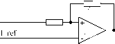
15.00 20.00 25.00 30.00 Time (ms) 35.00 40.00 FIGURE 12.42 PWM phase voltages: (a) PWM phase modulation; (b) PWM phase-to-phase voltage; and (c) PWM phase-to-neutral voltage. respectively. In a less straightforward fashion, the phase-to-neutral voltage can be evaluated with the help of Eq. (12.53): ¥wm - 1/3(wm ~ PWm) (12.53) where Vy is the phase-to-neutral voltage for phase a, and PWM phase-to-phase voltage between phase j and phase k. Figure 12.42 shows the PWM patterns for the phase-to-phase and phase-to-neutral voltages. 12.3.4 Control of the DC Link Voltage Control of dc link voltage requires a feedback control loop. As already explained in Section 12.3.2, the dc voltage Vp, is compared with a reference Vref d the error signal e obtained from this comparison is used to generate a template waveform. The template should be a sinusoidal waveform with the same frequency of the mains supply. This template is used to produce the PWM pattern, and allows controlhng the rectifier in two different ways: 1) as a voltage-source, current-controlled PWM rectifier; or 2) as a voltage-source, voltage-controlled PWM rectifier. The first method controls the input current, and the second controls the magnitude and phase of the voltage Vyq). The current controlled method is simpler and more stable than the voltage-controlled method, and for these reasons it will be explained first. V = Msin (Ot 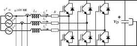 line(a) I line(b) I line(c) PWM generation Synchr. 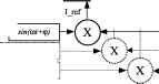 f >\ sin(fiit+(\20°) ~ >i sin((ia+(7A0°) FIGURE 12.43 Voltage-source current-controlled PWM rectifier. ence template i is evaluated by using the following equation: (12.54) Where Gq is shown in Fig. 12.43, and represents a controller such as PI, P, Fuzzy or other. The sinusoidal waveform of the template is obtained by multiplying i with a sine function, with the same frequency of the mains, and with the desired phase-shift angle (p, as shown in Fig. 12.43. Further, the template must be synchronized with the power supply. After that, the template has been created, and it is ready to produce the PWM pattern. Fiowever, one problem arises with the rectifier because the feedback control loop on the voltage Vc can produce instability. Then it becomes necessary to analyze this problem during rectifier design. Upon introducing the voltage feedback and the Gq controller, the control of the rectifier can be represented in a block diagram in Laplace dominion, as shown in Fig. 12.44. This block diagram represents a linearization of the system around an operating point, given by the rms value of the input current /5. The blocks Gi(S) and G2(S) in Fig. 12.44 represent the transfer function of the rectifier (around the operating point), and the transfer function of the dc link capacitor C, respectively Gi(S) = = 3 . (Vcos Ф - IRIs - LshS) (12.55) Als(S) GiS) = AV(S) APi(S)-AP2(5) Vp,-Cd-S (12.56) 12.3.4.1 Voltage-Source Current-Controlled PWM Rectifier This method of control is shown in the rectifier in Fig. 12.43. Control is achieved by measuring the instantaneous phase currents and forcing them to follow a sinusoidal current reference template I ref. The amplitude of the current refer-
G2(S) FIGURE 12.44 Close-loop rectifier transfer function. where APi(S) and AP2(S) represent the input and output power of the rectifier in Laplace dominion, V the rms value of the mains voltage supply (phase-to-neutral), Ig the input current being controUed by the template, Lg the input inductance, and R the resistance between the converter and power supply. According to stabihty criteria, and assuming a PI controUer, the foUowing relations are obtained: 3Kp Lg Kp V cos cp 2R-Kp + Ls- Kj (12.57) (12.58) I line
 / hysteresis band adjust These two relations are useful for the design of the current-controUed rectifier. They relate the values of dc link capacitor, dc link voltage, rms voltage supply, input resistance and inductance, and input power factor, with the rms value of the input current /5. With these relations the proportional and integral gains Kp and Kj can be calculated to ensure stability of the rectifier. These relations only estabhsh hmitations for rectifier operation, because negative currents always satisfy the inequalities. With these two stabUity limits satisfied, the rectifier wiU keep the dc capacitor vohage at the value of VpF (PI controller), for aU load conditions, by moving power from the ac to the dc side. Under inverter operation, the power wiU move in the opposite direction. Once the stabUity problems have been solved, and the sinusoidal current template has been generated, a modulation method wiU be required to produce the PWM pattern for the power valves. The PWM pattern wiU switch the power valves to force the input currents I line to follow the desired current template I ref. There are many modulation methods in the literature, but three methods for voltage source current controlled rectifiers are the most widely used ones: periodical sampling (PS); hysteresis band (HB); and triangular carrier (TC). The PS method switches the power transistors of the rectifier during the transitions of a square wave clock of fixed frequency: the periodical sampling frequency. In each transition, a comparison between I ref and I line is made, and corrections take place. As shown in Fig. 12.45a, this type of control is very simple to implement: only a comparator and a D-type flip-flop are needed per phase. The main advantage of this method is that the minimum time between switching transitions is limited to the period of the sampling clock. However, the actual switching frequency is not clearly defined. The HB method switches the transistors when the error between I ref and I line exceeds a fixed magnitude: the hysteresis band. As can be seen in Fig. 12.45b, this type of control needs a single comparator with hysteresis per phase. In this case the switching frequency is not determined, but its IJine I err 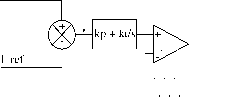 V tri FIGURE 12.45 Modulation control methods: (a) periodical sampling; (b) hysteresis band; and (c) triangular carrier. maximum value can be evaluated through the foUowing equation: cmax (12.59) where h is the magnitude of the hysteresis band. The TC method shown in Fig. 12.45c, compares the error between I ref and IJine with a triangular wave. This triangular wave has fixed amplitude and frequency and is caUed the triangular carrier. The error is processed through a proportional-integral (PI) gain stage before comparison with the triangular carrier takes place. As can be seen, this control scheme is more complex than PS and HB. The values for kp and ki determine the transient response and steady-state error of the TC method. It has been found empirically that the values for kp and ki shown in Eqs. (12.60) and (12.61) give a good dynamic performance under several operating conditions: CO, ki = (D kp* (12.60) (12.61) where is the total series inductance seen by the rectifier, is the triangular carrier frequency, and is the dc link voltage of the rectifier. In order to measure the level of distortion (or undesired harmonic generation) introduced by these three control methods, Eq. (12.62) is defined: % Distortion = 100 1 (%ne - hdfdt (12.62) In Eq. (12.62), the term Irms is the effective value of the desired current. The term inside the square root gives the rms value of the error current, which is undesired. This formula measures the percentage of error (or distortion) of the generated waveform. This definition considers the ripple, amplitude, and phase errors of the measured waveform, as opposed to the THD, which does not take into account offsets, scalings, and phase shifts. Figure 12.46 shows the current waveforms generated by the three forementioned methods. The example uses an average switching frequency of 1.5 kFiz. The PS is the worst, but its implementation is digitally simpler. The FiB method and TC with PI control are quite similar, and the TC with only proportional control gives a current with a small phase shift. Fiowever, Fig. 12.47 shows that the higher the switching frequency, the closer the results obtained with the different modulation methods. Over 6 kFiz of switching frequency, the distortion is very small for all methods. 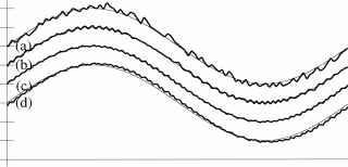 FIGURE 12.46 Waveforms obtained using 1.5 kHz switching frequency and Ls = U mH: (a) PS method; (b) HB method; (c) TC method {kp + ki); and (d) TC method (kp only). # 4 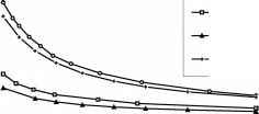 - Periodical Sampling - Hysteresis Band - Triangular Carrier (kp*+ki*) - Triangular Carrier (only kp*) 1000 2000 3000 4000 5000 Switching Frequency (Hz) 6000 7000 FIGURE 12.47 Distortion comparison for a sinusoidal current reference. 12.3.4.2 Voltage-Source Voltage-Controlled PWM Rectifier Figure 12.48 shows a one-phase diagram from which the control system for a voltage-source voltage-controlled rectifier is derived. This diagram represents an equivalent circuit of the fundamentals, that is, pure sinusoidal at the mains side, and pure dc at the dc link side. The control is achieved by creating a sinusoidal voltage template Vqd which is modified in amplitude and angle to interact with the mains vohage V. In this way the input currents are controlled without measuring them. The template Vjqd generated using the differential equations that govern the rectifier. The following differential equation can be derived from Fig. 12.48: v(t) = Ls + Ris + VyioD(t) (12.63) Assuming that v(t) = Ул/2 sin cot, then the solution for i(t), to acquire a template Vyq) able to make the rectifier work at constant power factor should be of the form: U0 = WOsin(a;t + (p) (12.64) Equations (12.63), (12.64), and v(t) allow a function of time able to modify Vmod amplitude and phase that will make the rectifier work at a fixed power factor. Combining these equations with v(t) yields %od(0 vv2 + Xsl sin cp - (rI, + L, cos Ф + i/, + L sin cp cos cp sm cot cos cot (12.65) Equation (12.65) provides a template for Vmod which is controlled through variations of the input current amplitude Jjax- The derivatives of 1 into Eq. (12.65) make sense, because 4 changes every time the dc load is modified. The term Xg in Eq. (12.65) is coLg. This equation can also be 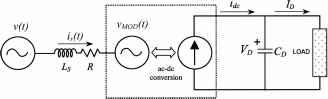 SOURCE RECTIFIER LOAD FIGURE 12.48 One-phase fundamental diagram of the voltage-source rectifier. written for unity power factor operation. In such a case cos (p = ly and sin cp = 0: Vmod(0 = (vV2 - RI - Ls sin cot -XsIJ cos cot (12.66) With this last equation, a unity power factor, voltage source, voltage controlled PWM rectifier can be implemented as shown in Fig. 12.49. It can be observed that Eqs. (12.65) and (12.66) have an in-phase term with the mains supply (sin cot), and an in-quadrature term (cos cot). These two terms aUow the template Vyq) to change in magnitude and phase so as to have fuU unity power factor control of the rectifier. Compared with the control block of Fig. 12.43, in the voltage-source voltage-controUed rectifier of Fig. 12.49, there is no need to sense the input currents. However, to ensure StabUity limits as good as the hmits of the current-controUed rectifier, blocks -R-sL and -Xg in Fig. 12.49 have to emulate and reproduce exactly the real values of R, X, and of the power circuit. However, these parameters do not remain constant, and this fact affects the stability of this system, making it less stable than the system shown in Fig. 12.43. In theory, if the impedance parameters are reproduced exactly, the stability limits of this rectifier are given by the same equations as used for the current-controlled rectifier seen in Fig. 12.43 (Eqs. (12.57) and (12.58). Under steady-state, i is constant, and Eq. (12.66) can be written in terms of phasor diagram, resulting in Eq. (12.67). As shown in Fig. 12.50, different operating conditions for the unity power factor rectifier can be displayed with this equation: jcoLsIs 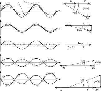 FIGURE 12.50 Steady-state operation of the unity power factor rectifier, under different load conditions. With the sinusoidal template Vjy[od already created, a modulation method to commutate the transistors wiU be required. As in the case of the current-controlled rectifier, there are many methods to modulate the template, with the most weU known the so-caUed sinusoidal pulse width modulation (SPWM), which uses a triangular carrier to generate the PWM as shown in Fig. 12.51. Only this method wiU be described in this chapter. comparator = V-RIs-jX,Is (12.67) Vmod Vtriang  VpwM 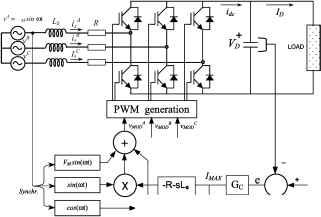 vref FIGURE 12.49 Implementation of the voltage-controlled rectifier for unity power factor operation. 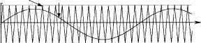 Vtriang Vmod VpwM Vpwm Ш Time (ms) FIGURE 12.51 Sinusoidal modulation method based on triangular carrier. 1 ... 17 18 19 20 21 22 23 ... 91 |
||||||||||||||||||||||||||||||||||||||||||||||||||||||||||||||||||||||||||||||||||||||||||||||||||||||||||||||||||||||||||||||||||||||||||||||||||||||||||
|
© 2026 AutoElektrix.ru
Частичное копирование материалов разрешено при условии активной ссылки |