 |
 |
 |
| Главная Журналы Популярное Audi - почему их так назвали? Как появилась марка Bmw? Откуда появился Lexus? Достижения и устремления Mercedes-Benz Первые модели Chevrolet Электромобиль Nissan Leaf |
Главная » Журналы » Metal oxide semiconductor 1 ... 19 20 21 22 23 24 25 ... 91 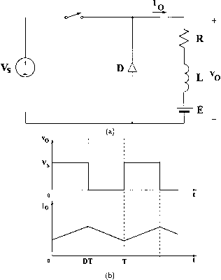 FIGURE 13.2 DC chopper with RLE load: (a) circuit diagram; (b) waveforms. FIGURE 13.3 The dc step-up chopper. 13.3 Step-Down (Buck) Converter 13.3.1 Basic Converter The step-down dc-dc converter, commonly known as a buck converter, is shown in Fig. 13.4a. It consists of dc input voltage source V5, controlled switch S, diode D, filter inductor L, filter capacitor C, and load resistance R. Typical waveforms in the converter are shown in Fig. 13.4b under the assumption that the inductor current is always positive. The state of the converter in which the inductor current is never zero for any period of time is called the continuous conduction mode 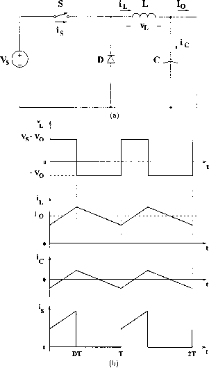 >R Vo FIGURE 13.4 Buck converter: (a) circuit diagram; (b) waveforms. (CCM). It can be seen from the circuit that when the switch S is commanded to the on state, the diode D is reverse-biased. When the switch S is off, the diode conducts to support an uninterrupted current in the inductor. The relationship among the input voltage, output voltage, and the switch duty ratio D can be derived, for instance, from the inductor voltage Vp waveform (see Fig. 13.4b). According to Faradays law, the inductor volt-second product over a period of steady-state operation is zero. For the buck converter {Vs-Vo)DT = -Vo{l-D)T (13.3) Fience, the dc voltage transfer function, defined as the ratio of the output voltage to the input voltage, is (13.4) It can be seen from Eq. (13.4) that the output voltage is always smaller that the input voltage. The dc-dc converters can operate in two distinct modes with respect to the inductor current i. Figure 13.4b depicts the CCM in which the inductor current is always greater than zero. When the average value of the output current is low (high R) and/or the switching frequency / is low, the converter may enter the discontinuous conduction mode (DCM). In the DCM, the inductor current is zero during a portion of the switching period. The CCM is preferred for high efficiency and good utilization of semiconductor switches and passive components. The DCM may be used in applications with special control requirements because the dynamic order of the converter is reduced (the energy stored in the inductor is zero at the beginning and at the end of each switching period). It is uncommon to mix these two operating modes because of different control algorithms. For the buck converter, the value of the filter inductance that determines the boundary between CCM and DCM is given by (1 - m (13.5) For typical values of D = 0.5, = 10 Q, and / = 100 kHz, the boundary is Ly = 25 iH. For L > Ly, the converter operates in the CCM. The filter inductor current ip in the CCM consists of a dc component Iq with a superimposed triangular ac component. Almost aU of this ac component flows through the filter capacitor as a current i. Current i causes a smaU voltage ripple across the dc output voltage Vq. To limit the peak-to-peak value of the ripple voltage below a certain value V, the filter capacitance С must be greater than С . - (1-D)Vq SV.LP (13.6) At D = 0.5, VJVq = 1%, L = 25 iH, and / = 100 kHz, the minimum capacitance is C = 25 iF. Equations (13.5) and (13.6) are the key design equations for the buck converter. The input and output dc voltages (hence, the duty ratio D), and the range of load resistances R are usually determined by preliminary specifications. The designer needs to determine values of passive components L and C, and of the switching frequency /. The value of the filter inductor L is calculated from the CCM/DCM condition using Eq. (13.5). The value of the filter capacitor С is obtained from the voltage ripple condition Eq. (13.6). For the compactness and low conduction losses of a converter, it is desirable to use smaU passive components. Equations (13.5) and (13.6) show that it can be accomplished by using a high switching frequency /. The switching frequency is limited, however, by the type of semiconductor switches used and by switching losses. It should also be noted that values of L and С may be altered by the effects of parasitic components in the converter, especially by the equivalent series resistance of the capacitor. Parasitic components in dc-dc converters are discussed in Section 13.7. 13.3.2 Transformer Versions of Buck Converter In many dc power supphes, a galvanic isolation between the dc or ac input and the dc output is required for safety and reliability. An economical means of achieving such an isolation is to employ a transformer version of a dc-dc converter. High-frequency transformers are of a small size and low weight and provide high efficiency. Their turns ratio can be used additionally to adjust the output voltage level. Among buck-derived dc-dc converters, the most popular are the forward converter, the push-puU converter, the half-bridge converter, and the full-bridge converter. 13.3.2.1 Forward Converter The circuit diagram of a forward converter is depicted in Fig. 13.5. When the switch S is on, diode conducts and diode D2 is off. The energy is transferred from the input, through the transformer, to the output filter. When the switch is off, the state of diodes and D2 is reversed. The dc voltage transfer function of the forward converter is My = -n (13.7) where n = N/N2. In the forward converter, the energy-transfer current flows through the transformer in one direction. Hence, an additional winding with diode D3 is needed to bring the magnetizing current of the transformer to zero, which prevents transformer saturation. The turns ratio М^/Щ should be selected in such a way that the magnetizing current decreases to zero during a fraction of the time interval when the switch is off. Equations (13.5) and (13.6) can be used to design the filter components. The forward converter is very popular for low-power applications. For medium-power levels, converters with bidirectional transformer excitation (push-puU, half-bridge, and full-bridge) are preferred due to better utihzation of magnetic components. 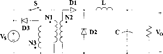 FIGURE 13.5 Forward converter. Dl L FIGURE 13.6 Push-pull converter. 13.3.2.2 Push-PuU Converter The PWM dc-dc push-puU converter is shown in Fig. 13.6. The switches and s2 operate shifted in phase by T/2 with the same duty ratio D, however, the duty ratio must be smaUer than 0.5. When switch is on, diode D conducts and diode D2 is off; the diode states are reversed when switch s2 is on. When both controllable switches are off, the diodes are on and share equally the filter inductor current. The dc voltage transfer function of the push-puU converter is (13.8) where n = N/N2. The boundary value of the filter inductor is (1 - 2D)R (13.9) The filter capacitor can be obtained from (1 - iDWo С - 32у,1/2 (13.10) 13.3.2.3 Half-Bridge Converter Figure 13.7 shows the dc-dc half-bridge converter. The operation of the PWM half-bridge converter is similar to that of the push-pull converter. In comparison to the push-puU converter. 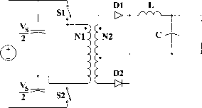 FIGURE 13.7 Half-bridge converter. S3\ S4 4>- FIGURE 13.8 Full-bridge converter. the primary switch of the transformer is simplified at the expense of two voltage-sharing input capacitors. The half-bridge converter dc voltage transfer function is My=-- = -Vc n (13.11) where D < 0.5. Equations (13.9) and (13.10) apply to the filter components. 13.3.2.4 Full-Bridge Converter Comparing the PWM dc-dc fuU-bridge converter of Fig. 13.8 to the half-bridge converter, it can be seen that the input capacitors have been replaced by two controUable switches that are operated in pairs. When and S4 are on, voltage V5 is applied to the primary switch of the transformer and diode D conducts. With s2 and S3 on, there is voltage - V5 across the transformer primary switch and diode D2 is on. With all controllable switches off, both diodes conduct in the same way as in the push-pull and half-bridge converters. The dc voltage transfer function of the fuU-bridge converter is Vn 2D (13.12) where D < 0.5. The values of filter components can be obtained from Eqs. (13.9) and (13.10). It should be stressed that the fuU-bridge topology is a very versatile one. With different control algorithms, it is very popular in dc-ac conversion (square-wave and PWM single-phase inverters), and it is also used in four-quadrant dc drives. 13.4 Step-Up (Boost) Converter Figure 13.9a depicts a step-up or a PWM boost converter. It consists of dc input voltage source V5, boost inductor L, controlled switch S, diode D, filter capacitor C, and load resistance R. The converter waveforms in the CCM are 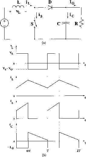 The boost converter operates in the CCM for L > Ц where О FIGURE 13.9 Boost converter: (a) circuit diagram; (b) waveforms. presented in Fig. 13.9b. When the switch S is in the on state, the current in the boost inductor increases linearly and the diode D is off at that time. When the switch S is turned off, the energy stored in the inductor is released through the diode to the output RC circuit. Using Faradays law for the boost inductor VsDT = (Vo - Vs)(l - D)T from which the dc voltage transfer function turns out to be (13.14) (1 - PfPR 2/ (13.15) For D = 0.5, = 10 Q, and / = 100 kHz, the boundary value of the inductance is = 6.25 iH. As shown in Fig. 13.9b, the current supphed to the output RC circuit is discontinuous. Thus, a larger filter capacitor is required in comparison to that in the buck-derived converters to hmit the output voltage ripple. The filter capacitor must provide the output dc current to the load when the diode D is off. The minimum value of the filter capacitance that results in the voltage ripple is given by V,Rf (13.16) At D = 0.5, VJVo = 1%, = 10 Q, and / = 100 kHz, the minimum capacitance for the boost converter is C = 50 iF. The boost converter does not have a popular transformer (isolated) version. 13.5 Buck-Boost Converter 13.5.1 Basic Converter A nonisolated (transformerless) topology of the buck-boost converter is shown in Fig. 13.10a. The converter consists of dc input voltage source V, controlled switch S, inductor L, diode D, filter capacitor C, and load resistance R. With the switch on, the inductor current increases while the diode is maintained off. When the switch is turned off, the diode provides a path for the inductor current. Note the polarity of the diode that results in its current being drawn from the output. The buck-boost converter waveforms are depicted in Fig. 13.10b. The condition of a zero volt-second product for the inductor in steady state yields VsDT =-Vo(l - D)T (13.17) (13.13) Hence, the dc voltage transfer function of the buck-boost converter is (13.18) The output voltage Vq is negative with respect to the ground. Its magnitude can be either greater or smaller (equal at As the name of the converter suggests, the output voltage is D = 0.5) than the input voltage as the name of the converter always greater than the input voltage. implies. 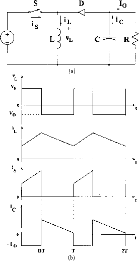 FIGURE 13.10 forms. Buck-boost converter: (a) circuit diagram; (b) wave- The value of the inductor that determines the boundary between the CCM and DCM is (1 - DfR 2/ The structure of the output part of the converter is similar to that of the boost converter (reversed polarities are the only difference). Thus, the value of the filter capacitor can be obtained from Eq. (13.16). 13.5.2 Flyback Converter A PWM flyback converter is a very practical isolated version of the buck-boost converter. The circuit of the flyback converter is presented in Fig. 13.11a. The inductor of the buck-boost converter has been replaced by a flyback transformer. The input dc source and switch S are connected in series with the transformer primary. The diode D and the RC output circuit are connected in series with the secondary of the flyback transformer. Figure 13.11b shows the converter with a simple flyback transformer model that includes a magnetizing inductance and an ideal transformer with a turns ratio n = NilN2. The flyback transformer leakage inductances and losses are neglected in the model. It should be noted that leakage inductances, although not important from the viewpoint of the principle of operation, affect adversely switch and diode transitions. Therefore, snubbers are usually required in flyback converters Refer to Fig. 13.11b for the converter operation. When the switch S is on, the current in the magnetizing inductance increases hnearly, the diode D is off and there is no current in the ideal transformer windings. When the switch is turned off, the magnetizing inductance current is diverted into the ideal transformer, the diode turns on, and the transformed magnetizing inductance current is supplied to the RC load. The dc voltage transfer function of the flyback converter is Vs n(l - D) (13.20) It differs from the buck-boost converter voltage transfer function by the turns ratio factor n. A positive sign has been obtained by an appropriate coupling of the transformer windings. Unlike in transformer buck-derived converters, the magnetizing inductance of the flyback transformer is an important design parameter. The value of the magnetizing inductance that determines the boundary between the CCM and DCM is given by mb - n\l - DfR (13.21) (13.19)  FIGURE 13.11 Flyback conveter: (a) circuit diagram; (b) circuit with a transformere model showing the magnetizing inductance L. The value of the filter capacitance can be calculated using Eq. (13.16). 13.6 Cuk Converter The circuit of the Cuk converter is shown in Fig. 13.12a. It consists of dc input voltage source V, input inductor L, controllable switch S, energy transfer capacitor Cp diode D, filter inductor l2, filter capacitor C, and load resistance R. An important advantage of this topology is a continuous current at both the input and the output of the converter. Disadvantages of the Cuk converter are a high number of reactive components and high current stresses on the switch, the diode, and the capacitor C. The main waveforms in the converter are presented in Fig. 13.12b. When the switch is on, the diode is off and the capacitor is discharged by the inductor L2 current. With the switch in the off state, the diode conducts currents of the inductors Ц and L2, whereas capacitor is charged by the inductor Ц current. To obtain the dc voltage transfer function of the converter, we shall use the principle that the average current through a capacitor is zero for steady-state operation. Let us assume that inductors Ц and L2 are large enough that their ripple current can be neglected. Capacitor is in steady state if IL2DT = - D)T (13.22) For a lossless converter Ps = Vshi =-Vohi = Po (13.23) Combining these two equations, the dc voltage transfer function of the Cuk converter is (13.24) This voltage transfer function is the same as that for the buck-boost converter. The boundaries between the CCM and DCM are determined by (1 - D)R 2Df (13.25) 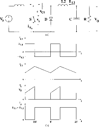 for Li and (1 - D)R 2/ (13.26) for L2. The output part of the Cuk converter is similar to that of the buck converter. Hence, the expression for the filter capacitor С is (1 - D)Vo (13.27) The peak-to-peak ripple voltage in the capacitor Cj can be estimated as (13.28) FIGURE 13.12 Cuk converter: (a) circuit diagram; (b) waveforms. A transformer (isolated) version of the Cuk converter can be obtained by splitting capacitor Cj and inserting a high-frequency transformer between the split capacitors. 13.7 Effects of Parasitics The analysis of converters in Sections 13.2 through 13.6 has been performed under ideal switch, diode, and passive component assumptions. Nonidealities or parasitics of practical devices and components may, however, greatly affect some performance parameters of dc-dc converters. In this section, the effects of parasitics on output voltage ripple, efficiency, and voltage transfer function of converters wiU be iUustrated. A more realistic model of a capacitor than simply a capacitance C, consists of a series connection of capacitance С and resistance r. The resistance is called an equivalent series resistance (ESR) of the capacitor and is due to losses in the dielectric and physical resistance of leads and connections. Recall Eq. (13.6) that provided a value of the filter capacitance in a buck converter that limits the peak-to-peak output voltage ripple to V. Equation (13.6) was derived under an assumption that the entire triangular ac component of the inductor current flows through a capacitance C. It is, however, closer to reality to maintain that this triangular component flows through a series connection of capacitance С and resistance r. The peak-to-peak ripple voltage is independent of the voltage across the filter capacitor and is determined only by the ripple voltage of the ESR if the foUowing condition is satisfied: 2гс/ 2гс/ (13.29) If condition Eq. (13.29) is satisfied, the peak-to-peak ripple voltage of the buck and forward converters is rcVo(l-DJ (13.30) For push-puU, half-bridge, and fuU-bridge converters, (13.31) 2гс/ 2гс/ where D < 0.5. If Eq. (13.31) is met, the peak-to-peak ripple voltage of these converters is given by rcVo(0.5-DJ (13.32) Waveforms of voltage acroos the ESR vq, voltage across the capacitance Vq, and total ripple voltage are depicted in Fig. 13.13 for three values of the filter capacitances. For the case of the top graph in Fig. 13.13, the peak-to-peak value of is higher than the peak-to-peak value of v because С < C. The middle and bottom graphs in Fig. 13.13 show the waveforms for С = Cjnin and С > Cjnin. respectively. For both these cases, the peak-to-peak voltages of and vc equal to each other. Note that when the resistance sets the ripple voltage V, the minimum value of inductance L is determined either by the boundary between the CCM and DCM according to Eq. (13.5) (buck and forward converters) or Eq. (13.9) (push-pull. 0.08 -0.08 0.08 -0.04 -0.08 0.08 -0.08
FIGURE 13.13 Voltage ripple waveforms vC, Vq, and for a buck converter at = 12 V, / = 100 kHz, L = 40 iH, = 0.05 Q and various values of C: С = 33 iF (top graph); С = C, = 65 iF (middle graph); and С = 100 jiF (bottom graph). half-bridge, and fuU-bridge converters), or by the voltage ripple condition Eq. (13.30) or (13.32). In buck-boost and boost converters, the peak-to-peak capacitor current Ipp is equal to the peak-to-peak diode current and is given by T - (13.33) under the condition that the inductor current ripple is much lower than the average value of the inductor current. The peak-to-peak voltage across the ESR is V - r T - (13.34) Assuming that the total ripple voltage is approximately equal to the sum of the ripple voltages across the ESR and the capacitance, the maximum value of the peak-to-peak ripple voltage across the capacitance is Cmax К - к. (13.35) Finally, by analogy to Eq. (13.16), when the ESR of the filter capacitor is taken into account in the boost-type output filter, the filter capacitance should be greater than (13.36) Parasitic resistances, capacitances, and voltage sources also affect the energy conversion efficiency of dc-dc converters. The efficiency rj is defined as a ratio of output power to the input power Vnl, (13.37) Thus as efficiencies are usually specified in percent, let us consider the boost converter as an example. Under the low ripple assumption, the boost converter efficiency can be estimated as R(l - Df R(l-D)\l + V/Vo+fC,R) + Drs + (1 - D)rr, + D(l - D)rc (13.38) where V, is the forward conduction voltage drop of the diode, Q is the output capacitance of the switch, Гр is the ESR of the inductor, and r, is the forward on resistance of the diode. The term fCR in Eq. (13.38) represents switching losses in the converter; other terms account for conduction losses. Losses in a dc-dc converter contribute also to a decrease in the dc voltage transfer function. The nonideal dc voltage transfer function My is a product of the ideal one and the efficiency (13.39) Sample graphs for the boost converter that correspond to Eqs. (13.38) and (13.39) are presented in Fig. 13.14. 13.8 Synchronous and Bidirectional Converters It can be observed in Eq. (13.38) that the forward voltage of a diode Vjj contributes to a decrease in efficiency. This contribution is especially significant in low-output voltage power supphes, for example, 3.3-V power supplies for microprocessors or power supplies for portable telecommunication equipment. Even with a Schottky diode, which has Vj) in the range of 0.4 V, the power loss in the diode can easily exceed 10% of 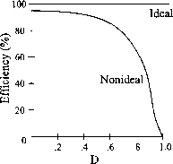 10 T 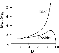 FIGURE 13.14 Effects of parasitics on characteristics of a boost converter: efficiency (top graph) and dc voltage transfer function (bottom graph). the total power delivered to the load. To reduce conduction losses in the diode, a low on-resistance switch can be added in parallel as shown in Fig. 13.15 for a buck converter. The input switch and the switch paraUel to the diode must be turned on and off alternately. The arrangement of Fig. 13.15 is called a synchronous converter or a synchronous rectifier. Modern low-voltage MOSFETs have on resistances of only several miUiohms. Hence, a synchronous converter may exhibit higher efficiency than a conventional one at output currents as large as tens of amperes. The efficiency is increased at the expense of a more complicated driving circuitry for the switches. In particular, a special care must be exercised to avoid having both switches on at the same time as this would 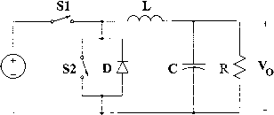 FIGURE 13.15 Synchronous buck converter. о FIGURE 13.16 Bidirectional flyback converter. short the input voltage source. As power semiconductor devices usually have longer turn-off times than turn-on times, a dead time (sometimes called a blanking time) must be introduced in PWM driving signals. The paraUel combination of a controUable switch and a diode is also used in converters, which aUow for a current flow in both directions - from the input source to the load and from the load back to the input source. Such converters are caUed bidirectional power-flow or simply bidirectional converters. As an example, a flyback bidirectional converter is shown in Fig. 13.16. It contains unipolar voltage and bidirectional current switch-diode combinations at both the primary switch and the secondary switch of the flyback transformer. When the primary switch and secondary diode operate, the current flows from the input source to the load. The converter current can also flow from the output to the input through the secondary switch and primary diode. Bidirectional arrangements can be made for both buck and boost converters. A bidirectional buck converter operates as a boost converter when the current flow is from the output to the input. A bidirectional boost converter operates as a buck converter with a reversed current flow. If for any reason (for instance, to avoid the DCM) the controllable switches are driven at the same time, they must be driven alternately with a sufficient dead time. 13.9 Control Principles A dc-dc converter must provide a regulated dc output voltage under varying load and input voltage conditions. The converter component values are also changing with time, temperature, pressure, and so forth. Fience, the control of the output voltage should be performed in a closed-loop manner using principles of negative feedback. The two most common closed-loop control methods for PWM dc-dc converters, namely, the voltage-mode control and the current-mode control, are presented schematically in Fig. 13.17. In the voltage-mode control scheme shown in Fig. 13.17a, the converter output voltage is sensed and subtracted from an external reference voltage in an error amplifier. The error amplifier produces a control voltage that is compared to a constant-amplitude sawtooth waveform. The comparator produces a PWM signal that is fed to drivers of controUable switches in the dc-dc converter. The duty ratio of the PWM signal depends on the value of the control voltage. The frequency of the PWM signal is the same as the frequency of the sawtooth waveform. An important advantage of the voltage-mode control is its simple hardware implementation and flexibility. The error amplifier in Fig. 13.17a reacts fast to changes in the converter output voltage. Thus, the voltage-mode control provides good load regulation, that is, regulation against variations in the load. Line regulation (regulation against variations in the input voltage) is, however, delayed because changes in the input voltage must first manifest themselves in the converter output before they can be corrected. To aUeviate this problem, the voltage-mode control scheme is sometimes augmented by a so-caUed voltage-feedforward path. The feedforward path affects directly the PWM duty ratio according to variations in the input voltage. As wiU be explained in what foUows, the input voltage feedforward is an inherent feature of current-mode control schemes. The current-mode control scheme is presented in Fig. 13.7b. An additional inner control loop feeds back an inductor current signal, and this current signal, converted into its voltage analog, is compared to the control voltage. This modification of replacing the sawtooth waveform of the voltage-mode control scheme by a converter current signal significantly alters the dynamic behavior of the converter, which then takes on some characteristics of a current source. Voltage reference 
Sawtooth waveform Output voltage Voltage reference  Control voltage Comparator and Latch PWM signal dc-dc Converter Switch or inductor current Output voltage FIGURE 13.17 Main control schemes for dc-dc converters: (a) voltage-mode control; (b) current-mode control. The output current in PWM dc-dc converters is either equal to the average value of the output inductor current (buck-derived and Cuk converters) or is a product of an average inductor current and a function of the duty ratio. In practical implementations of the current-mode control, it is feasible to sense the peak inductor current instead of the average value. As the peak inductor current is equal to the peak switch current, the latter can be used in the inner loop, which often simphfies the current sensor. Note that the peak inductor (switch) current is proportional to the input voltage. Hence, the inner loop of the current-mode control naturally accomphshes the input voltage-feedforward technique. Among several current-mode control versions, the most popular is the constant-frequency one that requires a clock signal. Advantages of the current-mode control are the input voltage feedforward, the hmit on the peak switch current, the equal current sharing in modular converters, and the reduction in the converter dynamic order. The main disadvantage of the current-mode control is its complicated hardware, which includes a need to compensate the control voltage by ramp signals (to avoid converter instability). Among other control methods of dc-dc converters, a hysteretic (or bang-bang) control is very simple for hardware implementation. However, the hysteretic control results in variable frequency operation of semiconductor switches. Generally, a constant switching frequency is preferred in power electronic circuits for easier ehmination of electromagnetic interference and better utilization of magnetic components. Application specific integrated circuits (ASICs) are commercially available that contain the main elements of voltage- or current-mode control schemes. On a single 14-or 16-pin chip, there is an error amplifier, comparator, sawtooth generator or sensed current input, latch, and PWM drivers. The switching frequency is usually set by an external RC network and can be varied from tens to hundreds of kilohertz. The controller has an oscillator output for synchronization with other converters in modular power supply systems, and a constant voltage reference is generated on the chip as weU. Additionally, the ASIC controller may be equipped with various diagnostic and protection features; for example, current limiting, overvoltage and undervoltage protection, soft start, dead time in case of multiple PWM outputs, and duty ratio hmiting. In several dc-dc converter topologies, for example, buck and buck-boost, neither control terminal of semiconductor switches is grounded (so-called high-side switches). The ASIC controUers are usually designed for a particular topology and their PWM drivers may be able to drive high-side switches in low-voltage applications. However, in high-voltage applications, external PWM drivers must be used. External PWM drivers are also used for switches with high input capacitances. To take fuU advantage of the input-output isolation in transformer versions of dc-dc converters, such an isolation must be also provided in the control loop. Signal transformers or optocouplers are used for isolating feedback signals. Dynamic characteristics of closed-loop dc-dc converters must fulfiU certain requirements. To simphfy analysis, these requirements are usually translated into desired properties of the open loop. The open loop should provide a sufficient (typically, at least 45°) phase margin for stabUity, high bandwidth (about one-tenth of the switching frequency) for good transient response, and high gain (several tens of decibels) at low frequencies for small steady-state error. The open-loop dynamic characteristics are shaped by compensating networks of passive components around the error amplifier. Second- or third-order RC networks are commonly used. Because the converter itself is a part of the control loop, the design of compensating networks requires a knowledge of smaU-signal characteristics of the converter. There are several methods of smaU-signal characterization of PWM dc-dc converters, and the most popular ones provide average models of converters under the assumptions of high switching frequency. The averaged models are then linearized at an operating point to obtain smaU-signal transfer functions. Among analytical averaging methods, state-space averaging has been popular since the late 1970s. Circuit-based averaging is usually performed using PWM switch or direct replacement of semiconductor switches by controUed current and voltage sources. AU these methods can take into account converter parasitics. The most important smaU-signal characteristic is the control-to-output transfer function Tp. Other converter characteristics that are investigated are: the input-to-output (or line-to-output) voltage transfer function, also caUed the open-loop dynamic line regulation or the audio susceptibility, which describes the input-output disturbance transmission; the open-loop input impedance; and the open-loop dynamic load regulation. Buck-derived, boost, and buck-boost converters are second-order dynamic systems; the Cuk converter is a fourth-order system. Characteristics of buck and buck-derived converters are simUar to each other. Another group of converters with simUar smaU-signal characteristics is formed by boost, buck-boost, and flyback converters. Among parasitic components, the ESR of the filter capacitor introduces additional dynamic terms into transfer functions. Other parasitic resistances usually modify slightly the effective value of the load resistance. Sample characteristics in what foUows are given for nonzero r, neglecting other parasitics. The control-to-output transfer function of the forward converter is Us) d(s) V,Rrc s + l/Cr, nL(R + Гс) s+s(CRc+L)/LC(R+rc) + R/LC(R+rc) (13.40) 1 ... 19 20 21 22 23 24 25 ... 91 |
|||||||||||||||||||||||||||||||||||||||||||||||||||||||||||||||||||||||||||||||||||||||||||||||||||||||||
|
© 2026 AutoElektrix.ru
Частичное копирование материалов разрешено при условии активной ссылки |