 |
 |
 |
| Главная Журналы Популярное Audi - почему их так назвали? Как появилась марка Bmw? Откуда появился Lexus? Достижения и устремления Mercedes-Benz Первые модели Chevrolet Электромобиль Nissan Leaf |
Главная » Журналы » Metal oxide semiconductor 1 ... 20 21 22 23 24 25 26 ... 91 It can be seen that this transfer function has two poles and one zero. The zero is due to the filter capacitor ESR. Buck-derived converters can easily be compensated for stability with second-order controllers. The control-to-output transfer function of the boost converter is given by Us) = - (s+l/Crc)(s-(l-DfR/L) 52 + 5((1 - DfCRrc + L)/LC(R + Гс) +(1 - DfR/LC(R + Гс) (13.41) The zero -(1 - D)i/L is located in the right-half of the 5-plane Therefore, the boost converter (as well as buck-boost and flyback converters) is a nonminimum phase system. Nonminimum phase dc-dc converters are typically compensated with third-order controUers. Step-by-step procedures for the design of compensating networks are usually given by manufacturers of ASIC controllers in application notes. This section ends with a word on the behavior of dc-dc converters in distributed power supply systems. An important feature of closed-loop regulated dc-dc converters is that they exhibit a negative input resistance. As the load voltage is kept constant by the controUer, the output power changes with the load. With slow load changes, an increase (decrease) in the input voltage results in a decrease (increase) in the input power. This negative resistance property must be carefully examined during the system design to avoid resonances. 13.10 Applications of DC-DC Converters Step-down choppers find most of their applications in high-performance dc drive systems, for example, electric traction, electric vehicles, and machine tools. The dc motors with their winding inductances and mechanical inertia act as filters resulting in high-quality armature currents. The average output voltage of step-down choppers is a linear function of the switch duty ratio. Step-up choppers are used primarily in radar and ignition systems. The dc choppers can be modified for two-quadrant and four-quadrant operation. Two-quadrant choppers may be a part of autonomous power supply systems that contain battery packs and such renewable dc sources as photovoltaic arrays, fuel cells, or wind turbines. Four-quadrant choppers are applied in drives in which regenerative breaking of dc motors is desired, for example, transportation systems with frequent stops. The dc choppers with inductive outputs serve as inputs to current-driven inverters. The addition of filtering reactive components to dc choppers results in PWM dc-dc converters. The dc-dc converters can be viewed as dc transformers that deliver to the load a dc voltage or current at a different level than the input source. This dc transformation is performed by electronic switching means, not by electromagnetic means such as in conventional transformers. The output voltages of dc-dc converters range from one volt for special VLSI circuits to tens of kilo volts in X-ray lamps. The most common output voltages are: 3.3 V for modern microprocessors; 5 and 12 V for logic circuits; 48 V for telecommunication equipment; and 270 V for main dc bus on airplanes. Typical input voltages include 48 V, 170 V (the peak value of a 120-V rms line), and 270 V. Selection of a topology of dc-dc converters is determined not only by input/output voltages, which can be additionally adjusted with the turns ratio in isolated converters, but also by power levels, voltage and current stresses of semiconductor switches, and utilization of magnetic components. The low part-count flyback converter is popular in low power applications (up to 200 W). Its main deficiencies are a large size of the flyback transformer core and high voltage stress on the semiconductor switch. The forward converter is also a single switch converter. Because its core size requirements are smaller, it is popular in low-medium- (up to several hundreds of watts) power apphcations. Disadvantages of the forward converter are the need for demagnetizing winding, and a high voltage stress on the semiconductor switch. The push-puU converter is also used at medium-power levels. Due to bidirectional excitation, the transformer size is smaU. An advantage of the push-pull converter is also a possibility to refer driving terminals of both switches to the ground, which greatly simplifies the control circuitry. A disadvantage of the push-pull converter is a potential core saturation in the case of asymmetry. The half-bridge converter has a similar range of applications as the push-puU converter. There is no danger of transformer saturation in the half-bridge converter. It requires, however, two additional input capacitors to split in half the input dc source. The full-bridge converter is used at high (several kilowatts) power and voltage levels. The voltage stress on power switches is limited to the input voltage source value. A disadvantage of the fuU-bridge converter is a high number of semiconductor devices. The dc-dc converters are building blocks of distributed power supply systems in which a common dc bus voltage is converted to various other voltages according to requirements of particular loads. Such distributed dc systems are common in space stations, ships and airplanes, as weU as in computer and telecommunication equipment. It is expected that modern portable wireless communication and signal processing systems wiU use variable supply voltages to minimize power consumption and to extend battery hfe. Low-output voltage converters in these applications utilize the synchronous rectification arrangement. Another major area of dc-dc converter applications is related to the utility ac grid. For critical loads, if the utility grid fails, there must be a backup source of energy, for example, a battery pack. This need for continuous power delivery gave rise to various types of uninterruptible power supplies (UPSs). Thus dc-dc converters are used in UPSs to adjust the level of a rectified grid voltage to that of the backup source. Because during normal operation the energy flows from the grid to the backup source and during emergency conditions the backup source must supply the load, bidirectional dc-dc converters are often used. Moreover dc-dc converters are also used in dedicated battery chargers. Power electronic loads, especially those with front-end rectifiers, pollute the ac grid with odd harmonics. Thus dc-dc converters are used as intermediate stages, just after a rectifier and before the load-supplying dc-dc converter, for shaping the input ac current to improve power factor and decrease the harmonic content. The boost converter is especially popular in such power factor correction (PFC) applications. Another utility grid-related application of dc-dc converters is in interfaces between ac networks and dc renewable energy sources such as fuel ceUs and photovoltaic arrays. In isolated dc-dc converters, multiple outputs are possible with additional secondary windings of transformers. Only one output is regulated with a feedback loop, but other outputs depend on the duty ratio of the regulated one and on their loads. A multiple-output dc-dc converter is a convenient solution in applications where there is a need for one closely regulated output voltage and for one or more other noncritical output voltage levels. References 1. R. R Severns and G. Bloom, Modern DC-to-DC Switchmode Power Converter Circuits, Van Nostrand Reinhold Company, New York, 1985. 2. M. H. Rashid, Power Electronics, 2nd ed., Prentice-Hall, Englewood Cliffs, NJ, 1993. 3. N. Mohan, T. M. Undeland, and W. P. Robbins, Power Electronics: Converters, Applications and Design, 2nd ed., John Wiley & Sons, New York, 1995. 4. R. Erickson, Fundamentals of Power Electronics, Chapman and Hall, New York, 1997. 5. D. W. Hart, Introduction to Power Electronics, Prentice-Hall, Englewood Cliffs, NJ, 1997. 6. P. T. Krein, Elements of Power Electronics, Oxford University Press, ??????, 1998. 7. A. I. Pressman, Switching Power Supply Design, 2nd ed., McGraw-Hill, New York, 1998. 8. A. M. Trzynadlowski, Introduction to Modern Power Electronics, Wiley Interscience, New York, 1998. Inverters Jose R. Espinoza, Ph.D. Depto. Ing. ElectTica, Of. 220 Universidad de Concepcion Casilla 160-C, Correo 3 Concepcion, CHILE 14.1 14.2 14.3 14.4 14.5 14.6 14.7 14.8 Introduction...................................................................................... 225 Single-Phase Voltage Source Inverters.................................................... 227 14.2.1 Half-Bridge VSI 14.2.2 Full-Bridge VSI Three-Phase Voltage Source Inverters..................................................... 235 14.3.1 Sinusoidal PWM 14.3.2 Square-Wave Operation of Three-Phase VSls 14.3.3 Selective Harmonic Elimination in Three-Phase VSls 14.3.4 Space-Vector-Based Modulating Techniques 14.3.5 DC Link Current in Three-Phase VSls 14.3.6 Load-Phase Voltages in Three-Phase VSls Current Source Inverters...................................................................... 241 14.4.1 Carrier-based PWM Techniques in CSls 14.4.2 Square-Wave Operation of Three-Phase CSls 14.4.3 Selective Harmonic Elimination in Three-Phase CSls 14.4.4 Space-Vector-Based Modulating Techniques in CSls 14.4.5 DC Link Voltage in Three-Phase CSls Closed-Loop Operation of Inverters...................................................... 250 14.5.1 Feedforward Techniques in Voltage Source Inverters 14.5.2 Feedforward Techniques in Current Source Inverters 14.5.3 Feedback Techniques in Voltage Source Inverters 14.5.4 Feedback Techniques in Current Source Inverters Regeneration in Inverters..................................................................... 256 14.6.1 Motoring Operating Mode in Three-Phase VSls 14.6.2 Regenerative Operating Mode in Three-Phase VSls 14.6.3 Regenerative Operating Mode in Three-Phase CSls Multistage Inverters............................................................................. 260 14.7.1 Multicell Topologies 14.7.2 Multilevel Topologies Acknowledgments............................................................................... 267 References.......................................................................................... 267 14.1 Introduction The main objective of static power converters is to produce an ac output waveform from a dc power supply. These are the types of waveforms required in adjustable speed drives (ASDs), uninterruptible power supplies (UPS), static var compensators, active filters, flexible ac transmission systems (FACTS), and voltage compensators, which are only a few apphcations. For sinusoidal ac outputs, the magnitude, frequency, and phase should be controUable. According to the type of ac output waveform, these topologies can be considered as voltage source inverters (VSls), where the independently controUed ac output is a voltage waveform. These structures are the most widely used because they naturally behave as voltage sources as required by many industrial applications, such as adjustable speed drives (ASDs), which are the most popular application of inverters; see Fig. 14.1a. Similarly, these topologies can be found as current source inverters (CSls), where the independently controlled ac output is a current waveform. These structures are stiU widely used in medium-voltage industrial applications, where high-quality voltage waveforms are required. Static power converters, specifically inverters, are constructed from power switches and the ac output waveforms are therefore made up of discrete values. This leads to the generation of waveforms that feature fast transitions rather than smooth ones. For instance, the ac output voltage produced by the VSI of a standard ASD is a three-level 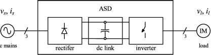
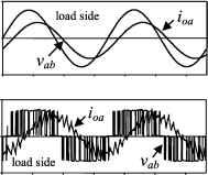 FIGURE 14.1 A standard adjustable speed drive scheme and associated waveforms: (a) the electrical power conversion topology; (b) the ideal input (ac mains) and output (load) waveforms; and (c) the actual input (ac mains) and output (load) waveforms. waveform (Fig. 14.1c). Although this waveform is not sinusoidal as expected (Fig. 14.1b), its fundamental component behaves as such. This behavior should be ensured by a modulating technique that controls the amount of time and the sequence used to switch the power valves on and off. The modulating techniques most used are the carrier-based technique (e.g., sinusoidal pulsewidth modulation, SPWM), the space-vector (SV) technique, and the selective-harmonic-elimination (SHE) technique. The discrete shape of the ac output waveforms generated by these topologies imposes basic restrictions on the applications of inverters. The VSI generates an ac output voltage waveform composed of discrete values (high dv/dt); therefore, the load should be inductive at the harmonic frequencies in order to produce a smooth current waveform. A capacitive load in the VSIs wiU generate large current spikes. If this is the case, an inductive filter between the VSI ac side and the load should be used. On the other hand, the CSI generates an ac output current waveform composed of discrete values (high di/dt); therefore, the load should be capacitive at the harmonic frequencies in order to produce a smooth voltage waveform. An inductive load in CSIs will generate large voltage spikes. If this is the case, a capacitive filter between the CSI ac side and the load should be used. A three-level voltage waveform is not recommended for medium-voltage ASDs due to the high dv/dt that would apply to the motor terminals. Several negative side effects of this approach have been reported (bearing and isolation problems). As alternatives to improve the ac output waveforms in VSIs are the multistage topologies (multilevel and multiceU). The basic principle is to construct the required ac output waveform from various voltage levels, which achieves medium-voltage waveforms at reduced dv/dt. Although these topologies are weU developed in ASDs, they are also suitable for static var compensators, active filters, and voltage compensators. Specialized modulating techniques have been developed to switch the higher number of power valves involved in these topologies. Among others, the carrier-based (SPWM) and SV-based techniques have been naturally extended to these applications. In many apphcations, it is required to take energy from the ac side of the inverter and send it back into the dc side. For instance, whenever ASDs need to either brake or slow down the motor speed, the kinetic energy is sent into the voltage dc link (Fig. 14.1a). This is known as the regenerative mode operation and, in contrast to the motoring mode, the dc link current direction is reversed due to the fact that the dc link voltage is fixed. If a capacitor is used to maintain the dc link voltage (as in standard ASDs) the energy must either be dissipated or fed back into the distribution system, otherwise, the dc hnk voltage gradually increases. The first approach requires the dc link capacitor be connected in parallel with a resistor, which must be properly switched only when the energy flows from the motor load into the dc hnk. A better alternative is to feed back such energy into the distribution system. However, this alternative requires a reversible-current topology connected between the distribution system and the dc hnk capacitor. A modern approach to such a requirement is to use the active front-end rectifier technologies, where the regeneration mode is a natural operating mode of the system. In this chapter, single and three-phase inverters in their voltage and current source alternatives will be reviewed. The dc link wiU be assumed to be a perfect dc, either voltage or current source that could be fixed as the dc link voltage in standard ASDs, or variable as the dc hnk current in some medium-voltage current source drives. Specifically, the topologies, modulating techniques, and control aspects, oriented to standard applications, are analyzed. In order to simplif) the analysis, the inverters are considered lossless topologies, which are composed of ideal power valves. Nevertheless, some practical nonideal conditions are also considered. 14.2 Single-Phase Voltage Source Inverters Single-phase voltage source inverters (VSls) can be found as half-bridge and full-bridge topologies. Although the power range they cover is the low one, they are widely used in power supphes, single-phase UPSs, and currently to form elaborate high-power static power topologies, such as for instance, the multicell configurations that are reviewed in Section 14.7. The main features of both approaches are reviewed and presented in the foUowing. 14.2.1 Half-Bridge VSI Figure 14.2 shows the power topology of a half-bridge VSI, where two large capacitors are required to provide a neutral point N, such that each capacitor maintains a constant voltage Vi/2. Because the current harmonics injected by the operation of the inverter are low-order harmonics, a set of large capacitors (C and C ) is required. It is clear that both switches and S cannot be on simultaneously because a short circuit across the dc link voltage source would be produced. There are two defined (states 1 and 2) and one undefined (state 3) switch state as shown in Table 14.1. In order to avoid the short circuit across the dc bus and the undefined ac output voltage condition, the modulating technique should always enure that at any instant either the top or the bottom switch of the inverter leg is on. TABLE 14.1 Switch states for a half-bridge single-phase VSI State State # Components Conducting
Figure 14.3 shows the ideal waveforms associated with the half-bridge inverter shown in Fig. 14.2. The states for the switches and S are defined by the modulating technique, which in this case is a carrier-based PWM. 14.2.1.1 The Carrier-Based Pulsewidth Modulation (PWM) Technique As mentioned earlier, it is desired that the ac output voltage 0 = aN follow a given waveform (e.g., sinusoidal) on a continuous basis by properly switching the power valves. The carrier-based PWM technique fulfils such a requirement as it defines the on and off states of the switches of one leg of a VSI by comparing a modulating signal (desired ac output voltage) and a triangular waveform 1;д (carrier signal). In practice, when > V/ the switch is on and the switch S is off; simUarly, when < V/ the switch is off and the switch S is on. A special case is when the modulating signal is a sinusoidal at frequency/ and amplitude v, and the triangular signal V/ is at frequency and amplitude йд. This is the sinusoidal PWM (SPWM) scheme. In this case, the modulation index (also known as the amplitude-modulation ratio) is defined as (14.1) and the normalized carrier frequency nif (also known as the frequency-modulation ratio) is v,/2 4=C + FIGURE 14.2 Single-phase half-bridge VSI. (14.2) Figure 14.3(e) clearly shows that the ac output voltage = v is basically a sinusoidal waveform plus harmonics, which features: (a) the amplitude of the fundamental component of the ac output voltage v satisf)ing the foUowing expression: (14.3) 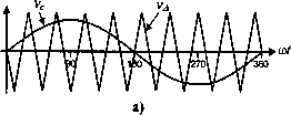 1 ю -v,/2 1 3 5 7 9 11 13 15 17 19 21 23 25 27 29 31 
1 3 5 7 9 11 13 15 17 19 21 23 25 27 29 31 FIGURE 14.3 The half-bridge VSL Ideal waveforms for the SPWM (m = 0.8, nif = 9): (a) carrier and modulating signals; (b) switch S+ state; (c) Switch S state; (d) ac output voltage; (e) ac output voltage spectrum; (f) ac output current; (g) dc current; (h) dc current spectrum; (i) switch current; (j) diode current. will be discussed later); (b) for odd values of the normalized carrier frequency the harmonics in the ac output voltage appear at normalized frequencies fr centered around and its multiples, specifically. h = lmf±k /=1,2,3,... (14.4) where /с = 2, 4, 6, ... for / = 1, 3, 5, ...; and /с = 1, 3, 5, ... for / = 2, 4, 6, ...; (с) the amplitude of the ac output voltage harmonics is a function of the modulation index and is independent of the normalized carrier frequency for nij: > 9; (d) the harmonics in the dc link current (due to the modulation) appear at normahzed frequencies fp centered around the normahzed carrier frequency and its multiples, specifically. p = lmf±k±l /=1,2,... (14.5) where /с = 2, 4, 6, ... for / = 1, 3, 5, ...; and /с = 1, 3, 5, ... for / = 2, 4, 6, Additional important issues are: (a) for smaU values of m (nif < 21) the carrier signal and the modulating signal should be synchronized to each other {mjr integer), which is required to hold the previous features; if this is not the case, subharmonics wiU be present in the ac output voltage; (b) for large values of (m > 21), the subharmonics are negligible if an asynchronous PWM linear regionN 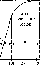 square wave ГПп FIGURE 14.4 Fundamental ac component of the output voltage in a half-bridge VSI SPWM modulated. technique is used, however, due to potential very low-order subharmonics, its use should be avoided; finally (c) in the overmodulation region (m > 1) some intersections between the carrier and the modulating signal are missed, which leads to the generation of low-order harmonics but a higher fundamental ac output voltage is obtained; unfortunately, the linearity between and achieved in the linear region Eq. (14.3) does not hold in the overmodulation region, moreover, a saturation effect can be observed (Fig. 14.4). The PWM technique aUows an ac output voltage to be generated that tracks a given modulating signal. A special case is the SPWM technique (the modulating signal is a sinusoidal) that provides in the linear region an ac output voltage that varies linearly as a function of the modulation index and the harmonics are at weU-defined frequencies and amplitudes. These features simplif) the design of filtering components. Unfortunately, the maximum amplitude of the fundamental ac voltage is vJ2 in this operating mode. Fiigher voltages are obtained by using the overmodulation region (m > 1); however, low-order harmonics appear in the ac output voltage. Very large values of the modulation index (m > 3.24) lead to a totally square ac output voltage that is considered as the square-wave modulating technique that is discussed in the next section. 14.2.1.2 Square-Wave Modulating Technique Both switches and S are on for one-half cycle of the ac output period. This is equivalent to the SPWM technique with an infinite modulation index m. Figure 14.5 shows the foUowing: (a) the normahzed ac output voltage harmonics are at frequencies /г = 3,5,7,9,..., and for a given dc link voltage; (b) the fundamental ac output voltage features an amplitude given by 4 V, and the harmonics feature an amplitude given by (14.6) (14.7) It can be seen that the ac output voltage cannot be changed by the inverter. Fiowever, it could be changed by controUing the dc link voltage v. Other modulating techniques that are applicable to half-bridge configurations (e.g., selective harmonic elimination) are reviewed here as they can easily be extended to modulate other topologies. 14.2.1.3 Selective Harmonic Elimination The main objective is to obtain a sinusoidal ac output voltage waveform where the fundamental component can be adjusted arbitrarily within a range and the intrinsic harmonics selectively eliminated. This is achieved by mathematically generating the exact instant of the turn-on and turn-off of the power valves. The ac output voltage features odd half- and quarter-wave symmetry; therefore, even harmonics are not present (vj = 0, h = 2, 4, 6, ...). Moreover, the per-phase voltage waveform (v = v in Fig. 14.2), should be chopped N times per half-cycle in order to adjust the fundamental and eliminate N - I harmonics in the ac output voltage waveform. For instance, to eliminate the third and fifth harmonics and to perform fundamental magnitude control (iV = 3), the equations to be solved are the foUowing: cos(lai) - cos(la2) + cos(la3) = (2 + nvi/Vi)/4: cos(3ai) - cos(3a2) + cos(3a3) = 1/2 cos(5ai) - cos(5a2) + cos(5a3) = 1/2 (14.8) where the angles a, and ot are defined as shown in Fig. 14.6a. The angles are found by means of iterative algorithms as no analytical solutions can be derived. The angles a, a2, and -Vi/2 ,3(0 I И M M M t t t t t t 1 3 5 7 9 11 13 15 17 19 21 23 25 27 29 31 a) b) FIGURE 14.5 The half-bridge VSI. Ideal waveforms for the square-wave modulating technique: (a) ac output voltage; (b) ac output voltage spectrum. Й Vo сц аво 4-v,/2  1 3 5 7 9 11 i3 15 i7 i9 21 23 25 27 29 31 0.8. 1 3 5 7 9 11 13 15 17 19 21 23 25 27 29 31 FIGURE 14.6 The half-bridge VSL Ideal waveforms for the SHE technique: (a) ac output voltage for third and fifth harmonic elimination; (b) spectrum of (a); (c) ac output voltage for third, fifth, and seventh harmonic elimination; (d) spectrum of (c). аз are plotted for different values of vJv in Fig. 14.7a. The fundamental magnitude control (N - I = 3), the equations general expressions to eliminate an even N - I to be solved are: (N-1=2,4,6,...) number of harmonics are k=l 4 / 1 - E(-l) cos(najt) = - for П = 3, 5, .. k=i 2 ., 2iV - 1 (14.9) cos(lai) - cos(la2) + cos(la3) - cos(la4) = (2 - nvi/vi)/4 cos(3ai) - cos(3a2) + cos(3a3) - cos(3a4) = 1/2 cos(5ai) - cos(5a2) + cos(5a3) - cos(5a4) = 1/2 cos(7ai) - cos(7a2) + cos(7a3) - cos(7a4) = 1/2 (14.10) where a, 1X2, ..., ot should satisfy < a2 < < as < where the angles a, a2, аз, and a4 are defined as shown in Fig. я/2. Similarly, to eliminate an odd number of harmonics, 14.6b. The angles ai,a2, аз and a4 are plotted for different for instance, the third, fifth and seventh, and to perform values of Si/i 14.7b. The general expressions to 100° 90° 80° 70° 60° 50° 40° 30° 20° 10° 0°
100° 90° 80° 70° 60° 50° 40° 30° 20° 10° 0°
FIGURE 14.7 Chopping angles for SHE and fundamental voltage control in half-bridge VSIs: (a) third and fifth harmonic elimination; (b) third, fifth, and seventh harmonic elimination. eliminate an odd N - 1 (iV - 1 = 3, 5, 7, ...) number of harmonics are given by -i:(-l)cos( a,)= k=i 4 1 1 - E(-l) cos(najt) = - for П = 3, 5,..., 2iV - 1 (14.11) where a, ..., as should satisf) < a2 < < as < 71/2. To implement the SHE modulating technique, the modulator should generate the gating pattern according to the angles as shown in Fig. 14.7. This task is usually performed by digital systems that normally store the angles in look-up tables. 14.2.1.4 DC Link Current The split capacitors are considered part of the inverter and therefore an instantaneous power balance cannot be considered due to the storage energy components (C+ and C ). Fiowever, if a lossless inverter is assumed, the average power absorbed in one period by the load must be equal to the average power supplied by the dc source. Thus, we can write v,(t) . i,(t) . dt = Vo(t) io(t) dt (14.12) where T is the period of the ac output voltage. For an inductive load and a relatively high switching frequency, the load current is nearly sinusoidal and therefore only the fundamental component of the ac output voltage provides power to the load. On the other hand, if the dc link voltage remains constant i;(t) = V, Eq. (14.12) can be simplified to 4(t)dt = - \fiVo\ sin(co/:) a/24 Mpot - Ф)- dt = Ц (14.13) where V is the fundamental rms ac output voltage, 4 is the rms load current, ф is an arbitrary inductive load power factor, and Ц is the dc link current that can be further simplified to Ц = 1соз(ф) (14.14) 14.2.2 Full-Bridge VSI Figure 14.8 shows the power topology of a fuU-bridge VSI. This inverter is similar to the half-bridge inverter; however, a second leg provides the neutral point to the load. As expected, both switches S and Si (or S2+ and S2 ) cannot be on simultaneously because a short circuit across the dc link voltage source would be produced. There are four defined (states 1, 2, 3, and 4) and one undefined (state 5) switch states as shown in Table 14.2. The undefined condition should be avoided so as to be always capable of defining the ac output voltage. In order to avoid the short circuit across the dc bus and the undefined ac output voltage condition, the modulating technique should ensure that either the top or the bottom switch of each leg is on at any instant. It can be observed that the ac output voltage can take values up to the dc link value v, which is twice that obtained with half-bridge VSI topologies. Several modulating techniques have been developed that are applicable to fuU-bridge VSls. Among them are the PWM (bipolar and unipolar) techniques. v,(J) FIGURE 14.8 Single-phase full-bridge VSI. TABLE 14.2 Switch states for a full-bridge single-phase VSI
14.2.2.1 Bipolar PWM Technique States 1 and 2 (Table 14.2) are used to generate the ac output voltage in this approach. Thus, the ac output voltage waveform features only two values, which are and -v. To generate the states, a carrier-based technique can be used as in half-bridge configurations (Fig. 14.3), where only one sinusoidal modulating signal has been used. It should be noted that the on state in switch S+ in the half-bridge corresponds to both switches S and being in the on state in the fuU-bridge configuration. Similarly, S in the on state in the half-bridge corresponds to both switches Si and being in the on state in the fuU-bridge configuration. This is caUed bipolar carrier-based SPWM. The ac output voltage waveform in a fuU-bridge VSI is basically a sinusoidal waveform that features a fundamental component of amplitude vi that satisfies the expression (14.15) in the linear region of the modulating technique (m < 1), which is twice that obtained in the half-bridge VSI. Identical conclusions can be drawn for the frequencies and amplitudes of the harmonics in the ac output voltage and dc link current, and for operations at smaUer and larger values of odd (including the overmodulation region (m > 1)), than in half-bridge VSIs, but considering that the maximum ac output voltage is the dc hnk voltage v. Thus, in the overmodulation region the fundamental component of amplitude v satisfies the expression (14.16) 14.2.2.2 Unipolar PWM Technique In contrast to the bipolar approach, the unipolar PWM technique uses the states 1, 2, 3, and 4 (Table 14.2) to generate the ac output voltage. Thus, the ac output voltage waveform can instantaneously take one of three values, namely, v, -v, and 0. To generate the states, a carrier-based technique can be used as shown in Fig. 14.9, where two sinusoidal modulating signals (v and -v) are used. The signal is used to generate v, and -v is used to generate Vy; thus Vy = -v. On the other hand, v = v - Vy = 2 v; thus vi = 2 vi = v. This is called unipolar carrier-based SPWM. Identical conclusions can be drawn for the amplitude of the fundamental component and harmonics in the ac output voltage and dc link current, and for operations at smaUer and larger values of trip (including the overmodulation region (Шд > 1)), than in full-bridge VSIs modulated by the bipolar SPWM. However, because the phase voltages (v and Vy) are identical but 180° out of phase, the output voltage (v = vy = v - Vy) wiU not contain even harmonics. Thus, if is taken even, the harmonics in the ac output voltage appear at normalized odd frequencies fr centered around twice the normalized carrier frequency and its multiples. Specifically, h = lmf±k / = 2,4,... (14.17) where к = 1, 3, 5, ... and the harmonics in the dc link current appear at normalized frequencies fp centered around twice the normalized carrier frequency and its multiples. Specifically, p = lmf±k±l 1 = 2,4,... (14.18) where к =1,3, 5, This feature is considered to be an advantage because it aUows the use of smaUer filtering components to obtain high-quality voltage and current waveforms whUe using the same switching frequency as in VSIs modulated by the bipolar approach. 14.2.2.3 Selective Harmonic Elimination In contrast to half-bridge VSIs, this approach is applied in a per-hne fashion for fuU-bridge VSIs. The ac output voltage features odd half- and quarter-wave symmetry; therefore, even harmonics are not present (й^ = 0, h = 2, 4, 6, ...). Moreover, the ac output voltage waveform (v = vy in Fig. 14.8), should feature N pulses per half-cycle in order to adjust the fundamental component and eliminate N - 1 harmonics. For instance, to eliminate the third, fifth and seventh harmonics and to perform fundamental magnitude control (iV = 4), the equations to be solved are: cos(lai) - cos(la2) + cos(la3) - cos(la4) = пЬКрА) cos(3ai) - cos(3a2) + cos(3a3) - cos(3a4) = 0 cos(5ai) - cos(5a2) + cos(5a3) - cos(5a4) = 0 cos(7ai) - cos(7a2) + cos(7a3) - cos(7a4) = 0 (14.19) where the angles a, a2, аз, and a4 are defined as shown in Fig. 14.10(a). The angles a, a2, аз, and a4 are plotted for different values of Voi/i 4- 14.11a. The general expressions to eliminate an arbitrary N - 1 {N - 1 = 3,5, 7,...) number of harmonics are given by -E(-ircos(na,) = - k=\ 4 Vi - E(-l) cos(najt) = 0 for П = 3, 5, ..., 2iV - 1 should satisfy a < ao < (14.20) where a, a2,... 71/2. Figure 14.10c shows a special case where only the fundamental ac output voltage is controUed. This is known as output control by voltage canceUation, which derives from the fact that its implementation is easily attainable by using two phase-shifted square-wave switching signals as shown in 1 ... 20 21 22 23 24 25 26 ... 91 |
||||||||||||||||||||||||||||||||||||||||||||||||||||||||||||||||||||||||||||||||||||||||||||||||||||||||||||||||||||||||||||||||||||||||||||||||||||||||||||||||||||||||||||||||||||||||||||||||||||||||||||||||||||||||||||
|
© 2026 AutoElektrix.ru
Частичное копирование материалов разрешено при условии активной ссылки |