 |
 |
 |
| Главная Журналы Популярное Audi - почему их так назвали? Как появилась марка Bmw? Откуда появился Lexus? Достижения и устремления Mercedes-Benz Первые модели Chevrolet Электромобиль Nissan Leaf |
Главная » Журналы » Metal oxide semiconductor 1 ... 21 22 23 24 25 26 27 ... 91 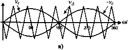   90 180 90 180 270 360 90 180 0.8v, I I I I I I I 1 I I I I I I I I 7- 1 3 5 7 9 11 13 15 17 19 21 23 25 27 29 31 90 180 I/ Z70 360 .....ft.H.ll.ll.ft, , >X 1 3 5 7 9 11 13 15 17 19 21 23 25 27 29 31 Л 270 360 FIGURE 14.9 The full-bridge VSI. Ideal waveforms for the unipolar SPWM (m = 0.8, lUf = 8): (a) carrier and modulating signals; (b) switch S state; (c) switch s2+ state; (d) ac output voltage; (e) ac output voltage spectrum; (f) ac output current; (g) dc current; (h) dc current spectrum; (i) switch current; (j) diode D current. ai аз Ш -V,-IT c) -t-O.Sv, 0.8v, I И И СИ Ф И t >-f 1 3 5 7 9 11 13 15 17 19 21 23 25 27 29 31 1 3 5 7 9 11 13 15 17 19 21 23 25 27 29 31 b) d) FIGURE 14.10 The half-bridge VSI. Ideal waveforms for the SHE technique: (a) ac output voltage for third, fifth, and seventh harmonic elimination; (b) spectrum of (a); (c) ac output voltage for fundamental control; (d) spectrum of (c). 100° 90° 80° 70° 60° 50° 40° 30° 20° 10° 0°
0 0.2 0.4 0.6 1.0 1.2 100° 90° 80° 70° 60° 50° 40° 30° 20° 10° 0°
0 0.2 0.4 0.6 FIGURE 14.11 Chopping angles for SHE and fundamental voltage control in half-bridge VSIs: (a) fundamental control and third, fifth, and seventh harmonic elimination; (b) fundamental control. Fig. 14.12. The phase-shift angle becomes 2 (Fig. 14.11b). Thus, the amplitude of the fundamental component and harmonics in the ac output voltage are given by oh = -v,jcos(hoi,), /z = 1, 3, 5, ... (14.21) n n It can also be observed in Fig. 14.12c that for = 0 square-wave operation is achieved. In this case, the fundamental ac output voltage is given by = -v (14.22) Ы.2.2Л DC Link Current Due to the fact that the inverter is assumed lossless and constructed without storage energy components, the instantaneous power balance indicates that v,(t) . i,(t) = vXt) Ш (14.23) For inductive load and relatively high switching frequencies, the load current is nearly sinusoidal. As a first approximation, the ac output voltage can also be considered sinusoidal. On the other hand, if the dc link voltage remains constant v-(t) = Vp Eq. (14.23) can be simplified to where the fundamental load voltage can be controUed by the manipulation of the dc link voltage. i,(t) = у sm(cDt) . sm(cDt - ф) (14.24)  0.8v, 180 270 360 1 3 5 7 9 11 13 15 17 19 21 23 25 27 29 31 b) d) FIGURE 14.12 The full-bridge VSI. Ideal waveforms for the output control by voltage cancellation: (a) switch state; (b) switch S2+ state; (c) ac output voltage; (d) ac output voltage spectrum. where V is the fundamental rms ac output voltage, 4 is the rms load current, and ф is an arbitrary inductive load power factor. Thus, the dc link current can be further simplified to = 4 со8(ф) - 4 cos(2a;t - ф) (14.25) The preceding expression reveals an important issue, that is, the presence of a large second-order harmonic in the dc link current (its amplitude is similar to the dc link current). This second harmonic is injected back into the dc voltage source, thus its design should consider it in order to guarantee a nearly constant dc link voltage. In practical terms, the dc voltage source is required to feature large amounts of capacitance, which is costly and demands space, both undesirable features, especially in medium- to high-power supphes. 14.3 Three-Phase Voltage Source Inverters Single-phase VSls cover low-range power apphcations and three-phase VSls cover the medium- to high-power applications. The main purpose of these topologies is to provide a three-phase voltage source, where the amplitude, phase, and frequency of the voltages should always be controUable. Although most of the apphcations require sinusoidal voltage waveforms (e.g., ASDs, UPSs, FACTS, var compensators), arbitrary voltages are also required in some emerging applications (e.g., active filters, voltage compensators). The standard three-phase VSI topology is shown in Fig. 14.13 and the eight valid switch states are given in Table 14.3. As in single-phase VSls, the switches of any leg of the inverter (Si and S4, S3 and S, or S5 and s2) cannot be switched on simultaneously because this would result in a short circuit across the dc hnk voltage supply. Similarly, in order to avoid undefined states in the VSI, and thus undefined ac output line voltages, the switches of any leg of the inverter cannot be switched off simultaneously as this will result in voltages that wiU depend upon the respective hne current polarity. Of the eight vahd states, two of them (7 and 8 in Table 14.3) produce zero ac line voltages. In this case, the ac line currents freewheel through either the upper or lower components. The 5. / A S, / FIGURE 14.13 Three-phase VSI topology. remaining states (1 to 6 in Table 14.3) produce nonzero ac output voltages. In order to generate a given voltage waveform, the inverter moves from one state to another. Thus the resulting ac output line voltages consist of discrete values of voltages that are v, 0, and -v for the topology shown in Fig. 14.13. The selection of the states in order to generate the given waveform is done by the modulating technique that should ensure the use of only the vahd states. 14.3.1 Sinusoidal PWM This is an extension of the one introduced for single-phase VSls. In this case and in order to produce 120° out-of-phase load voltages, three modulating signals that are 120° out of phase are used. Figure 14.14 shows the ideal waveforms of three-phase VSI SPWM. In order to use a single carrier signal and preserve the features of the PWM technique, the normalized carrier frequency should be an odd multiple of 3. Thus, all phase voltages {v, Vi,, and v) are identical but 120° out of phase without even harmonics; moreover, harmonics at frequencies a multiple of 3 are identical in amplitude and phase in aU phases. For instance, if the ninth harmonic in phase uN is a]V9(0 = Щ sin{9(Dt) (14.26) the ninth harmonic in phase hN wiU be Ш9(0 = Щ sin(9(a;t - 120°)) = Щ sm{9(Dt - 1080°) = Щ sm{9(Dt) (14.27) TABLE 14.3 Valild switch states for a three-phase VSI
 VabA -0.8-0.866-v, n n <-on -->С0/ 90 180 270 360 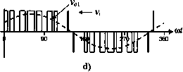 1 3 5 7 9 11 13 15 17 19 21 23 25 27 29 31 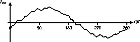 J /if1 J rifl Jl rifl Jri }а(\ )(Л( Л1111и11111Ш1111иТ11111Л11111Л1111 360 . . .ft. . .11. . j. . .fl. . л > 1 3 5 7 9 11 13 15 17 19 21 23 25 27 29 31 - 90 Ш 270 360 FIGURE 14.14 The three-phase VSL Ideal waveforms for the SPWM (m = 0.8, ruf = 9): (a) carrier and modulating signals; (b) switch state; (c) switch 5*3 state; (d) ac output voltage; (e) ac output voltage spectrum; (f) ac output current; (g) dc current; (h) dc current spectrum; (i) switch current; (j) diode current. Thus, the ac output line voltage vy = v - Vy wiU not contain the ninth harmonic. Therefore, for odd multiple of 3 values of the normalized carrier frequency т^, the harmonics in the ac output voltage appear at normalized frequencies fr centered around and its multiples, specifically, at h = lmf±k /=1,2,... (14.28) where / = 1, 3, 5, ... for /с = 2, 4, 6,..., and / = 2, 4, ... for k= 1, 5, 7, ..., such that h is not a multiple of 3. Therefore, the harmonics wiU be at ib 2, 2mf lb 5, ..., 3m lb 2, 3m ib 4, ..., mjr 4,..., Inif lb 1, Ami lb 1, Amf ±5, For nearly sinusoidal ac load current, the harmonics in the dc link current are at frequencies given by h = lmi±k±l /=1,2,... (14.29) where / = 0, 2, 4, ... for /с = 1, 5, 7, ..., and / = 1, 3, 5, ... for /с = 2, 4, 6, ..., such that h = I mj: ± к is positive and not a multiple of 3. For instance. Fig. 14.14h shows the sixth harmonic (h = 6), which is due to/z=l-9-2-l=6. The identical conclusions can be drawn for the operation at smaU and large values of m as for the single-phase configurations. However, because the maximum amplitude of the fundamental phase voltage in the linear region (w < 1) is 6406 the maximum amphtude of the fundamental ac output line voltage is й^ = \fbvill. Therefore, one can write that are inversely proportional to their harmonic order (Fig. 14.15d). Their amplitudes are О < < 1 (14.30) hn 2 (14.33) To further increase the amplitude of the load voltage, the amplitude of the modulating signal can be made higher than the amplitude of the carrier signal йд, which leads to overmodulation. The relationship between the amplitude of the fundamental ac output line voltage and the dc link voltage becomes nonlinear as in single-phase VSls. Thus, in the overmodulation region, the line voltages range in V3 < = £ 1 = £ 1 < - V3 (14.31) 2 я 2 14.3.2 Square-Wave Operation of Three-Phase VSls Large values of in the SPWM technique lead to full overmodulation. This is known as square-wave operation as illustrated in Fig. 14.15, where the power valves are on for 180°. In this operation mode, the VSI cannot control the load voltage except by means of the dc link voltage v. This is based on the fundamental ac line-voltage expression 71 2 (14.32) The ас hne output voltage contains the harmonics ff, where h = 6 k± I (/c = 1, 2, 3, ...) and they feature amplitudes 14.3.3 Selective Harmonic Elimination in Three-Phase VSls As in single-phase VSls, the SFLE technique can be apphed to three-phase VSls. In this case, the power valves of each leg of the inverter are switched so as to eliminate a given number of harmonics and to control the fundamental phase-voltage amplitude. Considering that in many applications the required line output voltages should be balanced and 120° out of phase, the harmonics multiple of three (/z = 3,9, 15,...), which could be present in the phase voltages (v, Vi,, and v), wiU not be present in the load voltages (i;, i;, and vJ. Therefore, these harmonics are not required to be eliminated, thus the chopping angles are used to eliminate only the harmonics at frequencies h = 5, 7, II, 13, ... as required. The expressions to eliminate a given number of harmonics are the same as those used in single-phase inverters. For instance, to eliminate the fifth and seventh harmonics and perform fundamental magnitude control (iV = 3), the equations to be solved are cos(lai) - cos(la2) + cos(la3) = (2 + nvJVi)/4 cos(5ai) - cos(5a2) + cos(5a3) = 1/2 (14.34) cos(7ai) - cos(7a2) + cos(7a3) = 1/2 where the angles a, and (X are defined as shown in Fig. 14.16a and plotted in Fig. 14.17. Figure 14.16b shows that the third, ninth, fifteenth,... harmonics are aU present in the phase voltages; however, they are not in the line voltages (Fig. 14.16d). 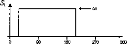 .360 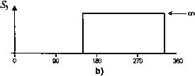 VabA. l.lv, I h И 11 >-f 1 3 5 7 9 11 13 15 17 19 21 23 25 27 29 31 ° FIGURE 14.15 The three-phase VSI. Square-wave operation: (a) switch state; (b) switch state; (c) ac output voltage; (d) ac output voltage spectrum. Уат ai аз 4-v,/2 1 3 5 7 9 11 13 15 17 19 21 23 25 27 29 31 -
0.8-v, to, J, 11 1.- 17 IQ 91 9fi 57 9Q 31 J* I I I I I 1 3 5 7 9 11 13 15 17 19 21 23 25 27 29 31 FIGURE 14.16 The three-phase VSL Ideal waveforms for the SHE technique: (a) phase voltage vj for fifth and seventh harmonic elimination; (b) spectrum of (a); (c) line voltage vjj for fifth and seventh harmonic elimination; (d) spectrum of (c). 14.3.4 Space-Vector-based Modulating Techniques At present, the control strategies are implemented in digital systems, and therefore digital modulating techniques are also available. The SV-based modulating technique is a digital technique in which the objective is to generate PWM load line voltages that are on average equal to given load line voltages. This is done in each sampling period by properly selecting the switch states from the valid ones of the VSI (Table 14.3) and by proper calculation of the period of times they are used. The selection and calculation times are based upon the space-vector transformation. 14.3.4.1 Space-Vector Transformation Any three-phase set of variables that add up to zero in the stationary abc frame can be represented in a complex plane by a complex vector that contains a real (a) and an imaginary () component. For instance, the vector of three-phase hne-modulating signals [ilabc = icacbccl t)e represented by the complex vector V, = [vi] = [саср] by means of the following transformation: сВ=(сЬ-сс) (14.35) (14.36) If the line-modulating signals [ilabc three balanced sinusoidal waveforms that feature an amplitude and an angular frequency ш, the resulting modulating signals in the (xP stationary frame V. = [v]f become a vector of fixed module v, which rotates at frequency ш (Fig. 14.18). Similarly, the SV transformation is applied to the hne voltages of 100° 90° 80° 70° 60° 50° 40° 30° 20° 10° 0° FIGURE 14.17 Chopping angles for SHE and fundamental voltage control in three-phase VSIs: fifth and seventh harmonic elimination. modulating vector Vc = [vjap sector number state 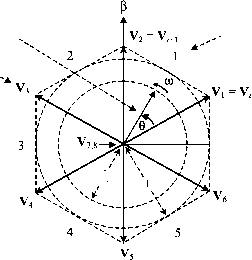 (6 )-► a FIGURE 14.18 The space-vector representation. the eight states of the VSI normahzed with respect to (Table 14.3), which generates the eight space vectors (V, i=l,2, ...,8) in Fig. 14.18. As expected, to are nonnuU line voltage vectors and Vy and Vg are nuU line-voltage vectors. The objective of the SV technique is to approximate the line-modulating signal space V. with the eight space vectors (y., i = 1, 2, ..., 8) available in VSls. Fiowever, if the modulating signal is laying between the arbitrary vectors V and Vi, only the nearest two nonzero vectors (V and V) and one zero SV (V = Vy or Vg) should be used. Thus, the maximum load line voltage is maximized and the switching frequency is minimized. To ensure that the generated voltage in one samphng period T (made up of the voltages provided by the vectors V, V, and V used during times T, T+j, and T) is on average equal to the vector V., the foUowing expression should hold: V,.T,=V,.T,+V (14.37) The solution of the real and imaginary parts of Eq. (14.37) for a line-load voltage that features an amplitude restricted to 0 <v <1 gives T- = TV, sm(n/3 - 9) 4+1 = T,-v,- sm(e) T=Z-Ъ-Ъ (14.38) (14.39) (14.40) The preceding expressions indicate that the maximum fundamental line-voltage amplitude is unity as 0 < 0 < я/3. This is an advantage over the SPWM technique which achieves a л/3/2 maximum fundamental hne-voltage amplitude in the linear operating region. Although, the SVM technique selects the vectors to be used and their respective on-times, the sequence in which they are used, the selection of the zero space vector, and the normalized sampled frequency remain undetermined. For instance, if the modulating line-voltage vector is in sector 1 (Fig. 14.18), the vectors V, V2, and V should be used within a samphng period by intervals given by Tp T2, and T, respectively. The question that remains is whether the sequence (i) Vj - V2 - V (ii) V, - Vj - V2 - V (iii) V, - Vl - V2 - Vl - V (iv) V, - Vl - V2 - V,-V2 - Vl - V, or any other sequence should actually be used. Finally, the technique does not indicate whether V should be V7, Vg, or a combination of both. 14.3.4.2 Space-Vector Sequences and Zero Space-Vector Selection The sequence to be used should ensure load line voltages that feature quarter-wave symmetry in order to reduce unwanted harmonics in their spectra (even harmonics). Additionally, the zero SV selection should be done in order to reduce the switching frequency. Although there is not a systematic approach to generate a SV sequence, a graphical representation shows that the sequence V, V+i, V (where V is alternately chosen among V7 and Vg) provides high performance in terms of minimizing unwanted harmonics and reducing the switching frequency. 14.3.4.3 The Normalized Sampling Frequency The normahzed carrier frequency in three-phase carrier-based PWM techniques is chosen to be an odd integer number multiple of 3 (m = 3 /7, /7 = 1, 3, 5, ...). Thus, it is possible to minimize parasitic or nonintrinsic harmonics in the PWM waveforms. A simUar approach can be used in the SVM technique to minimize uncharacteristic harmonics. Fience, it is found that the normalized sampling frequency should be an integer multiple of 6. This is due to the fact that in order to produce symmetrical line voltages, aU the sectors (a total of 6) should be used equally in one period. As an example. Fig. 14.19 shows the relevant waveforms of a VSI SVM for/ = 18 and = 0.8. Figure 14.19 confirms that the first set of relevant harmonics in the load line voltage are at which is also the switching frequency. 14.3.5 DC Link Current in Three-Phase VSls Due to the fact that the inverter is assumed to be lossless and constructed without storage energy components, the instantaneous power balance indicates that Vt) . lit) = V,y(t) . 4(0 + Vy,(t) . 4(0 + v (t) . i,(t) (14.41) where 4(0 4(0 4(0 re the phase-load currents as shown in Fig. 14.20. If the load is balanced and inductive, and a relatively high switching frequency is used, the load currents become nearly sinusoidal balanced waveforms. On the other hand, if the ac output voltages are considered sinusoidal and the dc link voltage is assumed constant Vi(t) = V-, Eq. (14.41) can be simplified to a/2\4i sin(a;0 V24 sm((Dt - ф) +л/2У,1 sin(a;t - 120°) v4 sin(a;t - 120° - ф) +л/2У,1 sin(a;t - 240°) л/24 sin(a;t - 240° - ф) (14.42) where \4i is the fundamental rms ac output line voltage, 4 is the rms load-phase current, and ф is an arbitrary inductive load power factor. Fience, the dc link current expression can be further simphfied to i,(t) = 34cos((/)) = V3/,cos((/)) (14.43) 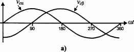 5. . Vabl ► CD? 90 180 270 360 ►со/ [пПППППН -0.8-V, /о 1ш 90 V 180  >(0t 90 180 270 360 т-г-rV-r-rii-r-r 1 3 5 7 9 11 13 15 17 19 21 23 25 27 29 31
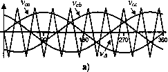
1 3 5 7 9 11 13 15 17 19 21 23 25 27 29 31 6 180 e) j) FIGURE 14.19 The three-phase VSL Ideal waveforms for space-vector modulation (v = 0.8,= 18): (a) modulating signals; (b) switch state; (c) switch state; (d) ac output voltage; (e) ac output voltage spectrum; (f) ac output current; (g) dc current; (h) dc current spectrum; (i) switch current; (j) diode current. v,/2iC+ Vi/2%C.  where Ij = лД is the rms load line current. The resulting dc hnk current expression indicates that under harmonic-free load voltages, only a clean dc current should be expected in the dc bus and, compared to single-phase VSIs, there is no presence of second harmonic. However, as the ac load line voltages contain harmonics around the normalized samphng frequency f, the dc link current wiU contain harmonics but around / as shown in Fig. 14.19h. 14.3.6 Load-Phase Voltages in Three-Phase VSIs FIGURE 14.20 Phase-load currents definition in a delta-connected The load is sometimes wye-connected and the phase-load load. voltages and v may be required (Fig. 14.21). To + Vab Vbc oc FIGURE 14.21 Phase-load voltages definition in a wye-connected load. obtain them, it should be considered that the line-voltage vector is
(14.44) which can be written as a fimction of the phase-voltage vector ian 4n cnV as. 1 -1 0 0 1 -1 -1 0 1 Expression (14.45) represents a linear system where the unknown quantity is the vector [v v. Unfortunately, the system is singular as the rows add up to zero (hne voltages add up to zero), therefore, the phase-load voltages cannot be obtained by matrix inversion. Fiowever, if the phase-load voltages add up to zero, Eq. (14.45) can be rewritten as
vom. 1 -1 0 0 1 -1 1 1 1 90 180 (14.46) Van A 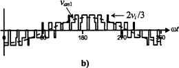 FIGURE 14.22 The three-phase VSI. Line- and phase-load voltages: (a) line-load voltage vi,; (b) phase-load voltage which is not singular and hence
1 -1 0 0 1 -1 1 1 1 2 1 1 -1 1 1 -1 -2 1 (14.47) that can be further simplified to
(14.48) The final expression for the phase-load voltages is only a function of vi, and i;, which is due to fact that the last row in Eq. (14.45) is chosen to be only ones. Figure 14.22 shows the line and phase-voltages obtained using Eq. (14.48). (14.45) 14,4 Current Source Inverters The main objective of these static power converters is to produce ac output current waveforms from a dc current power supply. For sinusoidal ac outputs, its magnitude, frequency, and phase should be controUable. Due to the fact that the ac line currents i, i, and (Fig. 14.23) feature high di/dt, a capacitive filter should be connected at the ac terminals in inductive load applications (such as ASDs). Thus, nearly sinusoidal load voltages are generated that justifies the use of these topologies in medium-voltage industrial applications, where high-quality voltage waveforms are required. Although single-phase CSls can in the same way as three-phase CSls topologies be developed under simUar principles, only three-phase apphcations are of practical use and are analyzed in the foUowing. In order to properly gate the power switches of a three-phase CSI, two main constraints must always be met: (a) the ac side is mainly capacitive, thus, it must not be short-circuited; this implies that, at most one top switch (1, 3, or 5 (Fig. 14.23)) and one bottom switch (4, 6, or 2 (Fig. 14.23)) с FIGURE 14.23 Three-phase CSI topology. TABLE 14.4 Valid switch states for a three-phase CSI
should be closed at any time; and (b) the dc bus is of the current-source type and thus it cannot be opened; therefore, there must be at least one top switch (1, 3, or 5) and one bottom switch (4, 6, or 2) closed at aU times. Note that both constraints can be summarized by stating that at any time, only one top switch and one bottom switch must be closed. There are nine valid states in three-phase CSIs. The states 7, 8, and 9 (Table 14.4) produce zero ac line currents. In this case, the dc link current freewheels through either the switches and S4, switches S3 and S, or switches S5 and s2. The remaining states (1 to 6 in Table 14.4) produce nonzero ac output line currents. In order to generate a given set of ac hne current waveforms, the inverter must move from one state to another. Thus, the resulting line currents consist of discrete values of current, which are 0, and -ц. The selection of the states in order to generate the given waveforms is done by the modulating technique that should ensure the use of only the valid states. Switching pulse generator Sal 4> 4> Shorting pulse distributor Sbl Shorting pulse generator I Scl 3> >c3 3> ООО Se3 Switching and shorting pulse combinator gating signals FIGURE 14.24 The three-phase CSI. Gating pattern generator for analog on-line carrier-based PWM. 1 ... 21 22 23 24 25 26 27 ... 91 |
|||||||||||||||||||||||||||||||||||||||||||||||||||||||||||||||||||||||||||||||||||||||||||||||||||||||||||||||||||||||||||||||||||||||||||||||||||||||||||||||||||||||||||||||||||||||||||||||||||||||||||||||||||||||||||||||||||||||||||||||||||||||||||||||||||||||||||||||||||||||||||||||||||||||||||||||||||||||||||||||||||||||||||||||||||||||||||||||||||||||||||||||||||
|
© 2026 AutoElektrix.ru
Частичное копирование материалов разрешено при условии активной ссылки |