 |
 |
 |
| Главная Журналы Популярное Audi - почему их так назвали? Как появилась марка Bmw? Откуда появился Lexus? Достижения и устремления Mercedes-Benz Первые модели Chevrolet Электромобиль Nissan Leaf |
Главная » Журналы » Metal oxide semiconductor 1 ... 22 23 24 25 26 27 28 ... 91 There are several modulating techniques that deal with the special requirements of CSls and can be implemented on line. These techniques are classified into three categories-(a) the carrier, (b) the selective harmonic elimination, and (c) the space-vector-based techniques. Although they are different, they generate gating signals that satisfy the special requirements of CSls. To simplify the analysis, a constant dc link current source is considered (ц = Ц). 14.4.1 Carrier-based PWM Techniques in CSls It has been shown that carrier-based PWM techniques that were initially developed for three-phase VSls can be extended to three-phase CSls. The circuit shown in Fig. 14.24 obtains the gating pattern for a CSI from the gating pattern developed for a VSI. As a result, the line current appears to be identical to the line voltage in a VSI for similar carrier and modulating signals. It is composed of a switching pulse generator, a shorting pulse generator, a shorting pulse distributor, and a switching and shorting pulse combinator. The circuit basically produces the gating signals ([S]i = [S ... S]) according to a carrier and three modulating signals [ilabc = iha kb ha\ Therefore, any set of modulating signals which when combined result in a sinusoidal line-to-line set of signals, wiU satisfy the requirement for a sinusoidal line current pattern. Examples of such a modulating signals are the standard sinusoidal, sinusoidal with third harmonic injection, trapezoidal, and deadband waveforms. The first component of this stage (Fig. 14.24) is the switching pulse generator, where the signals [Sy23 are generated according to: [5Jl23 = JHIGH = 1 if[abc>c I LOW = 0 otherwise (14.49) The outputs of the switching pulse generator are the signals [S]i 6, which are basically the gating signals of the CSI without the shorting pulses. These are necessary to freewheel the dc link current i when zero ac output currents are required. Table 14.5 shows the truth table of [S]i...6 for all combinations of their inputs [S[i23. It can be clearly seen that at most one top switch and one bottom switch is on, which satisfies the first constraint of the gating signals as stated before. In order to satisfy the second constraint, the shorting pulse (S = 1) is generated {shorting pulse generator (Fig. 14.24)) when none of the top switches (S = S = S = 0) or none of the bottom switches (S4 = S = = 0) are gated. Then, this pulse is added (using OR gates) to only one leg of the CSI (either to the switches 1 and 4, 3 and 6, or 5 and 2) by means of the switching and shorting pulse combinator (Fig. 14.24). The signals generated by the shorting pulse generator [Sy23 ensure TABLE 14.5 Truthtable for the switching pulse generator stage (Fig. 14.24) Top Switches Bottom Switches that: (a) only one leg of the CSI is shorted, as only one of the signals is high at any time; and (b) there is an even distribution of the shorting pulse, as [SJ123 is HIGH for 120° in each period. This ensures that the rms currents are equal in all legs. Figure 14.25 shows the relevant waveforms if a triangular carrier i and sinusoidal modulating signals [ilabc are used in combination with the gating pattern generator circuit (Fig. 14.24); this is SPWM in CSls. It can be observed that some of the waveforms (Fig. 14.25) are identical to those obtained in three-phase VSls, where a SPWM technique is used (Fig. 14.14). Specifically: (i) the load line voltage (Fig. 14.14d) in the VSI is identical to the load line current (Fig. 14.25d) in the CSI; and (n) the dc link current (Fig. 14.14g) in the VSI is identical to the dc link voltage (Fig. 14.25g) in the CSI. This brings up the duality issue between both topologies when similar modulation approaches are used. Therefore, for odd multiple of 3 values of the normalized carrier frequency mf, the harmonics in the ac output current appear at normalized frequencies ff centered around m and its multiples, specifically, at h = lmf±k /=1,2,... (14.50) where / = 1, 3, 5, ... for = 2, 4, 6, ... and / = 2, 4, ... for к = 1,5,7,..., such that h is not a multiple of 3. Therefore, the harmonics wiU be at mjr ±2, mjr ± 4,..., 2т^ ib 1, 2m lb 5,..., 3m ib 2, 3m ib 4, ..., 4mf ib 1, 4mf ±5, For nearly sinusoidal ac load voltages, the harmonics in the dc link voltage are at frequencies given by h=lmf±k±l /=1,2,... (14.51) where / = 0, 2, 4, ... for /с = 1, 5, 7, ..., and / = 1, 3, 5, ... for /с = 2, 4, 6, ..., such that h = I m ±kis positive and not a multiple of 3. For instance. Fig. 14.25h shows the sixth harmonic (h = 6), which is due to /г=1-9 - 2 - 1=6. Identical conclusions can be drawn for the operation at smaU and large values of m in the same way as for three-phase VSI configurations. Thus, the maximum amplitude of 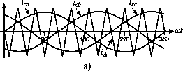 Joai <-on <-on ililHil -0.8-0.866i, 1 3 5 7 9 11 13 15 17 19 21 23 25 27 29 31  90 180 270 360 ...... I I I I I.....*i г 1 3 5 7 9 11 13 15 17 19 21 23 25 27 29 31 ° *<Sit FIGURE 14.25 The three-phase CSI. Ideal waveforms for the SPWM (m = 0.8, = 9): (a) carrier and modulating signals; (b) switch state; (c) switch 5*3 state; (d) ac output current; (e) ac output current spectrum; (f) ac output voltage; (g) dc voltage; (h) dc voltage spectrum; (i) switch Si current; (j) Switch Si voltage. the fundamental ac output line current is zj = л/Зц/2 and therefore one can write tnni = m, 0 <m<l (14.52) To further increase the amplitude of the load current, the overmodulation approach can be used. In this region, the fundamental line currents range in 4V3. 2 71 2 To further test the gating signal generator circuit (Fig. 14.24), a sinusoidal set with third and ninth harmonic injection modulating signals are used. Figure 14.26 shows the relevant waveforms. 14.4.2 Square-Wave Operation of Three-Phase CSIs As in VSIs, large values of in the SPWM technique lead to fuU overmodulation. This is known as square-wave operation. Figure 14.27 depicts this operating mode in a three-phase CSI, (14 53) power valves are on for 120°. As presumed, the CSI cannot control the load current except by means of the dc link 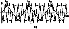 b) <-on 90 180 270 360 90 180 270 360 0 180 g) i> 90 4-on 90 180 270 360 Mil A0.8-0.866-i, I , , , И И Ь til >f 1 3 5 7 9 11 13 15 17 19 21 23 25 27 29 31 ° e) j) FIGURE 14.26 Gating pattern generator. Waveforms for third and ninth harmonic injection PWM (m = 0.8, = 15): signals as described in Figure 14.24. current Ц. This is due to the fact that the fundamental ac line current expression is . 4V3. The duality issue among both the three-phase VSI and CSI should be noted especially in terms of the line-load waveforms. The line-load voltage produced by a VSI is identical to the load line current produced by the CSI when both are (14.54) modulated using identical techniques. The next section wiU show that this also holds for SFiE-based techniques. The ac line current contains the harmonics ff, where h = 6 к ± I (/c=l,2,3,...), and they feature amplitudes that are inversely proportional to their harmonic order (Fig. 14.4.3 Selective Harmonic Elimination in 14.27d). Thus, oah -~~ 14л/3 . hn 2 Three-Phase CSls The SFiE-based modulating techniques in VSls define the (14 55) BB signals such that a given number of harmonics are eliminated and the fundamental phase-voltage amplitude is 0753 206017681153 5a ж <-on  so 18tf*J 270 Ileo 1.Ц I И I И 11. . >-f 180 270 360 1 3 5 7 9 11 13 15 17 19 21 23 25 27 29 31 b) d) FIGURE 14.27 The three-phase CSI. Square-wave operation: (a) switch Si state; (b) switch S state; (c) ac output current; (d) ac output current spectrum. controUed. If the required hne output vohages are balanced The circuit shown in Fig. 14.28 uses the gating signals and 120° out of phase, the chopping angles are used to developed for a VSI and a set of synchronizing signals [ijbc to ehminate only the harmonics at frequencies h = 5,7, obtain the gating signals [3] for a CSI. The synchronizing 11, 13, ... as required. signals [iJabc sinusoidal balanced waveforms that are Switching pulse generator gating signals 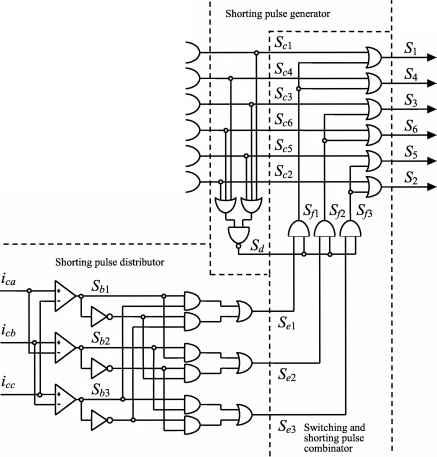 FIGURE 14.28 The three-phase CSI. Gating pattern generator for SHE PWM techniques. 100° 90° 80° 70° 60° 50° 40° 30° 20° 10° 0° FIGURE 14.29 Chopping angles for SHE and fundamental current control in three-phase CSls: fifth and seventh harmonic elimination. synchronized with the signals [SJ123 order to symmetrically distribute the shorting pulse and thus generate symmetrical gating patterns. The circuit ensures line current waveforms as the hne voltages in a VSI. Therefore, any arbitrary number of harmonics can be ehminated and the fundamental line current can be controlled in CSls. Moreover, the same chopping angles obtained for VSls can be used in CSls. For instance, to eliminate the fifth and seventh harmonics, the chopping angles are shown in Fig. 14.29, which are identical to that obtained for a VSI using Eq. (14.9). Figure 14.30 shows that the line current does not contain the fifth and the seventh harmonics as expected. Fience, any number of harmonics can be eliminated in three-phase CSls by means of the circuit (Fig. 14.28) without the hassle of how to satisfy the gating signal constrains. 14.4.4 Space-Vector-based Modulating Techniques in CSls The objective of the space vector (SV)-based modulating technique is to generate PWM load hne currents that are on average equal to given load line currents. This is done digitally in each samphng period by properly selecting the switch states from the valid ones of the CSI (Table 14.4) and the proper calculation of the period of times they are used. As in VSls, the selection and time calculations are based upon the space-vector transformation. 14.4.4.1 Space-Vector Transformation in CSls Similarly to VSls, the vector of three-phase line-modulating signals [ic[abc= ika hb hc\ п be represented by the complex vector = [iXp = [i, iff by means of Eqs. (14.35) and (14.36). For three-phase balanced sinusoidal modulating waveforms, which feature an amplitude and an angular frequency ш, the resuhing modulating signals complex vector Ic = Uc](xi5 becomes a vector of fixed module i, which rotates at frequency ш (Fig. 14.31). Similarly, the SV transformation is applied to the line currents of the nine states of the CSI normahzed with respect to which generates nine space vectors (Ip i = 1, 2, ..., 9 in Fig. 14.31). As expected, to 1б are nonnuU line current vectors and I7, Ig, and I9 are nuU line current vectors. The SV technique approximates the line-modulating signal spacevectorIcbyusingtheninespacevectors(I, i = 1, 2, ... ,9) available in CSls. If the modulating signal vector I. is between the arbitrary vectors and I, then and I combined with one zero SV (I = I7 or Ig or I9) should be used to generate I.. To ensure that the generated current in one sampling period T (made up of the currents provided by the vectors Ip I, and used during times T, T, and T) Sal A on 0.8-/i I I I I I 1 3 5 7 9 11 13 15 17 19 21 23 25 27 29 31 FIGURE 14.30 The three-phase CSI - ideal waveforms for the SHE technique: (a) VSI gating pattern for fifth and seventh harmonic elimination; (b) CSI gating pattern for fifth and seventh harmonic elimination; (c) line current i for fifth and seventh harmonic elimination; (d) spectrum of (c). 0733 modulating vector Ic = [/Jap state 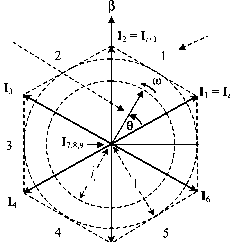 sector number FIGURE 14.31 The space-vector representation in CSIs. is on average equal to the vector I., the foUowing expressions should hold: T, = T,. i,. sin(/3 - в) Ti+i = T, i, sm(e) Т, = Т,- T, - T,+i (14.56) (14.57) (14.58) where 0 < < 1. Although, the SVM technique selects the vectors to be used and their respective on-times, the sequence in which they are used, the selection of the zero space vector, and the normahzed sampled frequency remain undetermined. 14.4.4.2 Space-Vector Sequences and Zero Space-Vector Selection Although there is no systematic approach to generate a SV sequence, a graphical representation shows that the sequence Ip Ii, I (where the chosen I depends upon the sector) provides high performance in terms of minimizing unwanted harmonics and reducing the switching frequency. To obtain the zero SV that minimizes the switching frequency, it is assumed that I. lays in Sector ф. Then Fig. 14.32 shows aU the possible transitions that could be found in Sector 2. It can be seen that the zero vector I9 should be chosen to minimize the switching frequency. Table 14.6 gives a summary of the zero space vector to be used in each sector in order to minimize the switching frequency. However, it should be noted that Table 14.6 is valid only for the sequence Ip I, I. Another sequence wiU require reformulating the zero space-vector selection algorithm. 14.4.4.3 The Normalized Sampling Frequency As in VSIs modulated by a space-vector approach, the normalized sampling frequency should be an integer multiple of 6 Initial state (a) Ii={l,2};*2. number of commutations (b) Ii={l,2};*2. Possible Zero Vector
>4 >4 Final state il2={2,3} t on switches minimum number of commutations --Ь={1,2} ;bb = {2,3} FIGURE 14.32 Possible state transitions in Sector (2) involving a zero SV. (a) Transition: I < I < I2 or I2 < I < Ii; (b) transition: I < I < I; (c) transition: I2 < I < I2. to minimize uncharacteristic harmonics. As an example. Fig. 14.33 shows the relevant waveforms of a CSI SVM for/ = 18 and = 0.8. Figure 14.33 also shows that the first set of relevant harmonics in the load line current are at 14.4.5 DC Link Voltage in Three-Phase CSIs An instantaneous power balance indicates that (14.59) where v(t), Vy(t), and v(t) are the phase filter voltages as shown in Fig. 14.34. If the filter is large enough and a relatively TABLE 14.6 Zero SV for minimum switching frequency in CSI and sequence/ /,+1,4
180 С)
-0.87i 1 3 5 7 9 11 13 15 17 19 21 23 25 27 29 31 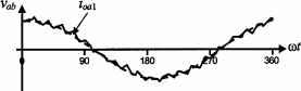 90 180 270 360 1 3 5 7 9 11 13 15 17 19 21 23 25 27 29 31 [1ГГ~П[1Г 11Л I 180 270 360 FIGURE 14.33 The three-phase CSI. Ideal waveforms for space-vector Modulation (z = 0.8, = 18): (a) modulating signals; (b) switch Si state; (c) switch state; (d) ac output current; (e) ac output current spectrum; (f) ac output voltage; (g) dc voltage; (h) dc voltage spectrum; (i) switch Si current; (j) Switch Si voltage. high switching frequency is used, the phase vohages become the ac output currents are considered sinusoidal and the dc nearly sinusoidal balanced waveforms. On the other hand, if link current is assumed constant i(t) = Eq. (14.59) can be simphfied to Vhr. ioc bn Vbc oc FIGURE 14.34 Phase voltage definition in a wye-connected filter. vit) = л/2У, sin(a;t) 21, sm(cDt - ф) +л/2У, sin(a;t - 120°) V2/,i sin(a;t - 120° - ф) +а/2У^ sm{cDt - 240°) a/2i sm{cDt - 240° - ф) (14.60) where is the rms ac output phase vohage, Ii is the rms fundamental line current, and ф is an arbitrary filter-load angle. Hence, the dc hnk voltage expression can be further simplified to the foUowing: Viit) = 3 y cos(<.) = V3 y cos(0) (14.61) where = а/З is the rms load line voltage. The resulting dc link voltage expression indicates that the first hne-current harmonic Ii generates a clean dc current. However, as the load line currents contain harmonics around the normalized sampling frequency the dc link current wiU contain harmonics but around as shown in Fig. 14.33h. Similarly, in carrier-based PWM techniques, the dc hnk current wiU contain harmonics around the carrier frequency (Fig. 14.25). In practical implementations, a CSI requires a dc current source that should behave as a constant (as required by PWM CSIs) or variable (as square-wave CSIs) current source. Such current sources should be implemented as separate units and they are described earlier in this book. inverters in the foUowing, although similar results are obtained for single-phase VSIs. 14.5.1 Feedforward Techniques in Voltage Source Inverters The dc link bus voltage in VSIs is usually considered a constant voltage source v. Unfortunately, and due to the fact that most practical applications generate the dc bus voltage by means of a diode rectifier (Fig. 14.35), the dc bus voltage contains low-order harmonics such as the sixth, twelfth,... (due to six-pulse diode rectifiers), and the second if the ac voltage supply features an unbalance, which is usually the case. Additionally, if the three-phase load is unbalanced, as in UPS applications, the dc input current in the inverter ц also contains the second harmonic, which in turn contributes to the generation of a second voltage harmonic in the dc bus. The basic principle of feedforward approaches is to sense the perturbation and then modify the input in order to compensate for its effect. In this case, the dc link voltage should be sensed and the modulating technique should accordingly be modified. The fundamental ab line voltage in a VSI SPWM can be written as 14.5 Closed-Loop Operation of Inverters Inverters generate variable ac waveforms from a dc power supply to feed, for instance, ASDs. As the load conditions usually change, the ac waveforms should be adjusted to these new conditions. Also, as the dc power supphes are not ideal and the dc quantities are not fixed, the inverter should compensate for such variations. Such adjustments can be done automatically by means of a closed-loop approach. Inverters also provide an alternative to changing the load operating conditions (i.e., speed in an ASD). There are two alternatives for closed-loop operation - the feedback and the feedforward approaches. It is known that the feedback approach can compensate for both perturbations (dc power variations) and load variations (load torque changes). However, the feedforward strategy is more effective in mitigating perturbations as it prevents its negative effects at the load side. These cause-effect issues are analyzed in three-phase (14.62) where is the carrier signal peak, vi and vi,i are the modulating signal peaks, and v (t) and v (t) are the modulating signals. If the dc bus voltage varies around a nominal V, value, then the fundamental line voltage varies proportionally; however, if the carrier signal peak г)д is redefined as Va = Уд, Vijt) (14.63) where Уд is the carrier signal peak (Fig. 14.36), then the resulting fiindamental ab line voltage in a VSI SPWM is VabM = \ ---f-\ (14.64) Diode Rectifier + Vab Vbc oc Lr bn figure 14.35 Three-phase topology with a diode-based front-end rectifier. TV. + у Am I-1 i -> \IVi <x)-> Carrier-based Modulation Teclinique FIGURE 14.36 The three-phase VSI. Feedforward control technique to reject dc bus voltage variations. where clearly the result does not depend upon the variations of the dc bus voltage. Fig. 14.37 shows the waveforms generated by the SPWM under a severe dc bus voltage variation (a second harmonic has been added manually to a constant V). As a consequence, the ac hne voltage generated by the VSI is distorted as it contains low-order harmonics (Fig. 14.37e). These operating conditions may not be acceptable in standard applications such as ASDs because the load wiU draw distorted three-phase currents as weU. The feedforward loop performance is illustrated in Fig. 14.38. As expected, the carrier signal is modified so as to compensate for the dc bus voltage variation (Fig. 14.38b). This is probed by the spectrum of the ac line voltage that does not contain low-order harmonics (Fig. 14.38e). It should be noted that > S, S; therefore, the compensation capabilities are limited by the required ac line voltage. The performance of the feedforward approach depends upon the frequency of the harmonics present in the dc bus voltage and the carrier signal frequency. Fortunately, the relevant unwanted harmonics to be found in the dc bus voltage are the second due to unbalanced supply voltages, and/or the sixth as the dc bus voltage is generated by means of a six-pulse diode rectifier. Therefore, a carrier signal featuring a 15-pu frequency is found to be sufficient to properly compensate for dc bus voltage variations. -I-r 270 360 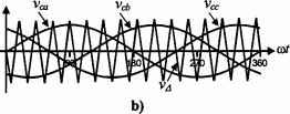 Va6A Vabl 90 Ш Ш -0.8-0.866-v, 1 3 5 J J.....И.4 9 11 13 15 17 19 21 23 25 27 29 31 FIGURE 14.37 The three-phase VSI. Ideal waveforms for regular SPWM {m = 0.8, mj = 9): (a) dc bus voltage; (b) carrier and modulating signals; (c) ac output voltage; (d) ac output voltage spectrum.  90 m < 0.8-0.866-v, 1 3 5 I T f I ( I I I I 9 11 13 15 17 19 21 23 25 27 29 31 FIGURE 14.38 The three-phase VSI. Ideal waveforms for SPWM including a feedforward loop {m = 0.8, mr = 9): (a) carrier and modulating signals; (b) Modified carrier and modulating signals; (c) ac output voltage; (d) ac output voltage spectrum. Unbalanced loads generate a dc input current ц that contains a second harmonic, which contributes to the dc bus voltage variation. The previous feedforward approach can compensate for such perturbation and maintain balanced ac load voltages. Digital techniques can also be modified in order to compensate for dc bus voltage variations by means of a feedforward approach. For instance, the SVM techniques indicate that the on-times of the vectors V V, and V are T,. = . i),. sin(/3 - в) Т, = Т,- T, - T,+i (14.65) (14.66) (14.67) respectively, where is the amplitude of the desired ac line voltage, as shown in Fig. 14.18. By redefining this quantity to 0<v, = V, < 1 (14.68) where is the nominal dc bus voltage and Vi(t) is the actual dc bus voltage. Thus, the on-times become T, = T,-v,ysm(n/3-e) (14.69) (14.70) (14.71) where v is the desired maximum ac line voltage. The previous expressions account for dc bus voltage variations and behave as a feedforward loop as it needs to sense the perturbation in order to be implemented. The previous expressions are valid for the linear region, thus is restricted to 0 < < 1, which indicates that the compensation is indeed limited. 14.5.2 Feedforward Techniques in Current Source Inverters The duality principle between the voltage and current source inverters indicates that, as described previously, the feedforward approach can be used for CSIs as well as for VSIs. Therefore, low-order harmonics present in the dc bus current can be compensated for before they appear at the load side. This can be done for both analog-based (e.g., carrier-based) and digital-based (e.g., space-vector) modulating techniques. 14.5.3 Feedback Techniques in Voltage Source Inverters Unlike the feedforward approach, the feedback techniques correct the input to the system (gating signals) depending upon the deviation of the output to the system (e.g., ac load hne currents in VSIs). Another important difference is that feedback techniques need to sense the controUed variables. In general, the controUed variables (output to the system) are chosen according to the control objectives. For instance, in ASDs, it is usually necessary to keep the motor line currents equal to a given set of sinusoidal references. Therefore, the controUed variables become the ac hne currents. There are several alternatives to implement feedback techniques in VSIs, and three of them are discussed in the foUowing. 14.5.3.1 Hysteresis Current Control The main purpose here is to force the ac line current to foUow a given reference. The status of the power valves and S4 are changed whenever the actual i current goes beyond a given reference i ib Ai/2. Figure 14.39 shows the hysteresis current controUer for phase a. Identical controUers are used in phase b and c. The implementation of this controUer is simple as it requires an op-amp operating in the hysteresis mode, thus the controUer and modulator are combined in one unit. Unfortunately, there are several drawbacks associated with the technique itself. First, the switching frequency cannot be predicted as in carrier-based modulators and therefore the harmonic content of the ac line voltages and currents becomes random (Fig. 14.40d). This could be a disadvantage when designing the filtering components. Second, as three-phase loads do not have the neutral connected as in ASDs, the load currents add up to zero. This means that only two ac line currents can be controUed independently at any given instant. Therefore, one of the hysteresis controUers is redundant at a given time. This explains why the load current goes beyond the hmits and introduces limit cycles (Fig. 14.40a). Finally, although the ac load currents add up to zero, the controllers cannot ensure that aU load line currents feature a zero dc component in one load cycle. 14.5.3.2 Linear Control of VSIs Proportional and proportional-integrative controUers can also be used in VSIs. The main purpose is to generate the modulating signals v, vy, and v in a closed-loop fashion I I oa.ref I - a phase a FIGURE 14.39 The three-phase VSI. Hysteresis current control (phase a). 1 ... 22 23 24 25 26 27 28 ... 91 |
||||||||||||||||||||||||||||||||||||||||||||||||||||||||||||||||||||||||||||||||||||||||||||||||||||||||||||||||||||||||||||||||||||||||||||||||||||||||||||||||||||||||||||||||||||||||||||||||||||||||||||||||||||||||||||||||||||||||||||||||
|
© 2026 AutoElektrix.ru
Частичное копирование материалов разрешено при условии активной ссылки |