 |
 |
 |
| Главная Журналы Популярное Audi - почему их так назвали? Как появилась марка Bmw? Откуда появился Lexus? Достижения и устремления Mercedes-Benz Первые модели Chevrolet Электромобиль Nissan Leaf |
Главная » Журналы » Metal oxide semiconductor 1 ... 23 24 25 26 27 28 29 ... 91 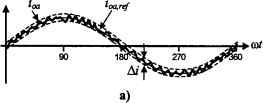 Vabl  0.8-0.866-v, i I I t , t t M 1 3 5 7 9 11 13 15 17 19 21 23 25 27 29 31 FIGURE 14.40 The three-phase VSI. Ideal waveforms for Hysteresis current control: (a) actual ac load current and reference; (b) Switch state; (c) ac output voltage; (d) ac output voltage spectrum. as depicted in Fig. 14.41. The modulating signals can be used by a carrier-based technique such as the SPWM (as depicted in Fig. 14.41) or by space-vector modulation. Because the load line currents add up to zero, the load line current references must add up to zero. Thus, the abc/ay transformation can be used to reduce to two controUers the overall implementation scheme as the у component is always zero. This avoids limit cycles in the ac load currents. The transformation of a set of variables in the stationary abc frame [x\ into a set of variables in the stationary frame [x\f is given by 1 i/2 -1/2 0 л/З/2 -л/3/2 (14.72) The selection of the controller (P, PI,...) is done according to control procedures such as steady-state error, settling time, overshoot, and so forth. Figure 14.42 shows the relevant waveforms of a VSI SPWM controUed by means of a PI controller as shown in Fig. 14.41. Although it is difficult to prove that no limit cycles are generated, the ac hne current appears very much sinusoidal. Moreover, the ac line voltage generated by the VSI preserves the characteristics of such waveforms generated by SPWM modulators. This is confirmed by the harmonic spectrum shown in Fig. 14.42d, where the first set of characteristic harmonics are around the normalized carrier frequency mjr = 15. Fiowever, an error between the actual i and the ac line current reference i can be observed (Fig. 14.42a). This error is inherent to linear controUers and cannot be totally eliminated, but it can be minimized by increasing the gain of the controller. Fiowever, the noise in the circuit is also increased, which could deteriorate the overaU performance of the control scheme. The inherent presence of the error in this type of controllers is due to the fact that the controUer needs a sinusoidal error to generate sinusoidal modulating signals v, vy, and v, as required by the modulator. Therefore, an error must exist between the actual and the ac line current references. Nevertheless, as current-controUed VSls are actually the inner loops in many control strategies, their inherent errors are compensated by the outer loop. This is the case of ASDs, where the outer speed loop compensates the inner current loops. In general, if the outer loop is implemented with dc quantities (such as speed), it can compensate the ac inner loops (such as ac line currents). If it is mandatory that a zero steady-state error be achieved with the ac quantities, then an stationary or rotating transformation is a valid alternative to use. 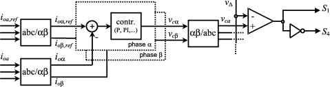 FIGURE 14.41 The three-phase VSI. Feedback control based on linear controllers. �44994 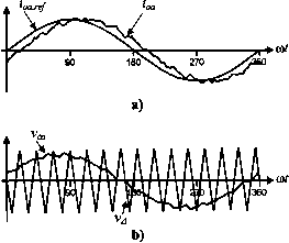 Vab a, yVabl -0.8-0.866-V, V/ ... I 1... и i 3 5 7 9 11 13 15 17 19 21 23 25 27 29 31 FIGURE 14.42 The three-phase VSL Ideal waveforms for a PI controller in a feedback loop (m =0.8, nif = 15): (a) actual ac load current and reference; (b) Carrier and modulating signals; (c) ac output voltage; (d) ac output voltage spectrum. 14.5.3.3 Linear Control of VSIs in Rotating Coordinates The direct-quadrature-zero (dqO) transformation aUows ac three-phase circuits to be operated as if they were dc circuits. This is based upon a mathematical operation that is the transformation of a set of variables in the stationary abc frame [x] into a set of variables in the rotating dqO frame [Idqo- The transformation is given by sin(a;t) cos(a;t) 1/V2 sin((jot - 2я/3) cos(a;t - 2я/3) 1/V2 sin((Dt - 4я/3) cos(a;t - 4я/3) 1/V2 labc (14.73) where ш is the angular frequency of the ac quantities. For instance, the current vector given by
loa,ref
dq/abc phase q becomes the vector FIGURE 14.43 The three-phase VSI. Feedback control based on dqO transformation. eliminated due to fact that the line currents at the load side add up to zero. The controllers in Fig. 14.43 include an integrator that generates the appropriate dc outputs and even if the actual and the line current references are identical. This ensures that zero steady-state error is achieved. The decoupling block in Fig. 14.43 is used to eliminate the cross-coupling effect generated by the dqO transformation and to allow an easier design of the parameters of the controllers. The dqO transformation requires the intensive use of multiplications and trigonometric functions. These operations can readily be done by means of digital microprocessors. Also, analog implementations would indeed be involved.
(14.75) where / and (p are the amplitude and phase of the line currents, respectively. It can be observed that: (a) the zero component Zq is always zero as the three-phase quantities add up to zero; and (b) the d and q components ij, are dc quantities. Thus, linear controllers should help to achieve zero steady-state error. The control strategy shown in Fig. 14.43 is an alternative where the zero-component controUer has been 14.5.4 Feedback Techniques in Current Source Inverters Duality indicates that CSIs should be controlled as equally as VSIs except that voltages become currents and currents become voltages. Thus, hystersis, linear and dq linear-based control strategies are also applicable to CSIs; however, the controUed variables are the load voltages instead of the load hne currents. For instance, the linear control of a CSI based on a dq transformation is depicted in Fig. 14.44. In this case, a passive balanced load is considered. In order to show that zero steady- 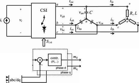
FIGURE 14.44 The three-phase CSI. Feedback control based on dqO transformation. State error is achieved, the per phase equations of the converter A first approximation is to assume that the decouphng are written as block is not there; in other words, = On the other hand, the model of the controUers can be written as c[tp]abc = [Uabc-Mabc [/]аЬс = [р]аЬс-ВДаЬс (14.76) (14.77) [Idq = {[p,re/]dq [pldql + ([p,re/]dq [pldq) (14.82) where к and T are the proportional and integrative gains of the ac line currents are in fact imposed by the modulator and the PI controUer that are chosen to achieve a desired dynamic they satisfy [olabc - i[c]abc response. Combining the model of the controUers and the model of the converter in dq coordinates and using the (14 78) Laplace transform, the following relationship between the reference and actual load-phase voltages is found: Replacing Eq. (14.78) into the model of the converter f. Г \ equations (14.76) and (14.77), using the dqO transformation [pldq ~ 7 and assuming nuU zero component, the model of the converter becomes [p,re/]dq (14.83) Ndq = -Mtpldq + -[dq [/Idq (14-79) In order to finally prove that zero steady-state error is - [i] = ] --[i] (14.80) achieved for step inputs in either the d or q component of L L the load-phase voltage reference, the previous expression is evaluated in 5 = 0. This results in the foUowing: where W is given by 0 -Ш Ш 0 Ndq=7 (14.81) = [p,re/]dq w + yj [p,re/]dq (14.84) As expected, the actual and reference values are identical. Finally, the relationship Eq. (14.83) is a matrix that is not diagonal. This means that both actual and reference load-phase voltages are coupled. In order to obtain a decoupled control, the decoupling block in Fig. 14.44 should be properly chosen. 14.6 Regeneration in Inverters Industrial applications are usually characterized by a power flow that goes from the ac distribution system to the load. This is, for example, the case of an ASD operating in the motoring mode. In this instance, the active power flows from the dc side to the ac side of the inverter. However, there are an important number of applications in which the load may supply power to the system. Moreover, this could be an occasional condition as weU a normal operating condition. This is known as the regenerative operating mode. For example, when an ASD reduces the speed of an electrical machine this can be considered a transient condition. DownhiU belt conveyors in mining applications can be considered a normal operating condition. In order to simplify the notation, it could be said that an inverter operates in the motoring mode when the power flows from the dc to the ac side, and in the regenerative mode when the power flows from the ac to the dc side. 14.6.1 Motoring Operating Mode in Three-Phase VSIs This is the case where the power flows from the dc side to the ac side of the inverter. Figure 14.45 shows a simphfied scheme of an ASD where the motor has been modeled by three RLe branches, where the sources [e\ are the back-emf. Because the ac hne voltages applied by the inverter are imposed by the pulsewidth-modulation technique being used, they can be adjusted according to specific requirements. In particular. Inn Va. h5> Diode Rectifier
R L lob Vbn Vbc С - -> I ОС Vcn c FIGURE 14.45 Three-phase VSI topology with a diode-based front-end rectifier. 0.667V, 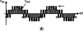
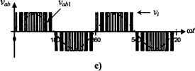 Pl a FIGURE 14.46 The ASD based on a VSI. Motoring mode: (a) dc bus voltage; (b) dc bus current; (c) ac line-load voltage; (d) ac phase-load voltage; (e) motor line current and back-emf; (f) shaft power. �2187700666666332111 Fig. 14.46 shows the relevant waveforms in steady state for the motoring operating mode of the ASD. To simplify the analysis, a constant dc bus voltage = has been considered. It can be observed that: (i) the dc bus current ц features a dc value Ц that is positive; and (ii) the motor line current is in phase with the back-emf. Both features confirm that the active power flows from the dc source to the motor. This also is confirmed by the shaft power plot (Fig. 14.46f), which is obtained as: Pi(t) = ea(t)iia(t) + ey(t)ijy(t) + e,(t)ij,(t) (14.85) 14.6.2 Regenerative Operating Mode in Three-Phase VSISs The back-emf sources [e\ are functions of the machine speed and as such they ideally change just as the speed changes. The regeneration operating mode can be achieved by properly modifying the ac line voltages applied to the machine. This is done by the speed outer loop that could be based on a scalar (e.g., V/f) or vectorial (e.g., field-oriented) control strategy. As indicated earlier, there are two cases of regenerative operating modes. 14.6.2.1 Occasional Regenerative Operating Mode This mode is required during transient conditions such as in occasional braking of electrical machines (ASDs). Specifically, the speed needs to be reduced and the kinetic energy is taken into the dc bus. Because the motor line voltage is imposed by the VSI, the speed reduction should be done in such a way that the motor line currents do not exceed the maximum values. This boundary condition wiU limit the ramp-down speed to a minimum, but shorter braking times wiU require a mechanical braking system. Figure 14.47 shows a transition from the motoring to regenerative operating mode for an ASD as shown in Fig. 14.45. Fiere, a stiff dc bus voltage has been used. Zone I in Fig. 14.47 is the motoring mode. Zone II is a transition condition, and Zone III is the regeneration mode. The line voltage is adjusted dynamically to obtain nominal motor hne currents during regeneration (Fig. 14.47d). Zone III clearly shows that the shaft power gets reversed. Occasional regeneration means that the drive rarely goes into this operating mode. Therefore, such energy can be: (a) left uncontrolled; or (b) burned in resistors that are paralleled to the dc bus. The first option is used in low- to medium-power applications that use diode-based front-end rectifiers. Therefore, the dc bus current flows into the dc bus capacitor and the dc bus voltage rises accordingly to Avi=IiAt (14.86) where Av is the dc bus voltage variation, С is the dc bus voltage capacitor, Ц is the average dc bus current during regeneration, and At is the duration of the regeneration operating mode. Usually, the drives have the capacitor С designed to allow a 10% overvoltage in the dc bus. The second option uses burning resistors R that are paralleled in the dc bus as shown in Fig. 14.48 by means of the switch Sj. A closed-loop strategy based on the actual dc bus voltage modifies the duty cycle of the turn-on/turn-off of the switch Sj in order to keep such voltage under to a given reference. This alternative is used when the energy recovered by the VSI would result in an acceptable dc bus voltage variation if an uncontrolled alternative is used. There are some special cases where the regeneration operating mode is frequently used. For instance, electrical shovels in mining companies have repetitive working cycles and 15% of the energy is sent back into the dc bus. In this case, a valid alternative is to send back the energy into the ac distribution system. The schematic shown in Fig. 14.49 is capable of taking the kinetic energy and sending it into the ac grid. As reviewed earlier, the regeneration operating mode reverses the polarity of the dc current and because the diode-based front-end converter cannot take negative currents, a thyristor-based front-end converter is added. Similarly to the burning-resistor approach, a closed-loop strategy based on the actual dc bus voltage Vl modifies the commutation angle a of the thyristor rectifier in order to keep such voltage under a given reference. 14.6.2.2 Regenerative Operating Mode as Normal Operating Mode Fewer industrial applications are capable of returning energy into the ac distribution system on a continuous basis. For instance, mining companies usually transport their product downhiU for few kilometers before processing it. In such cases, the drive maintains the transportation belt conveyor at constant speed and takes the kinetic energy. Due to the large amount of energy and the continuous operating mode, the drive should be capable of taking the kinetic energy, transforming it into electrical energy, and sending it into the ac distribution system. This would make the drive a generator that would compensate for the active power required by other loads connected to the electrical grid. The schematic shown in Fig. 14.50 is a modern alternative for adding regeneration capabilities to the VSI-based drive on a continuous basis. In contrast to the previous alternatives, this scheme uses a VSI topology as an active front-end converter, which is generally called a voltage-source rectifier VSR. The VSR operates in two quadrants, that is positive dc voltages and at positive/negative dc currents as reviewed earlier. This feature makes it a perfect match for ASDs based on a VSI. Some of the advantages of using a VSR topology are: (i) the ac supply current can be as sinusoidal as required (by increasing the switching frequency of the VSR or the ac line inductance); (ii) the operation can be done at a unity displacement power factor in both motoring and regenerative Zone II Zone III 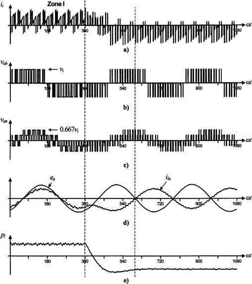 FIGURE 14.47 The ASD based on a VSL Motoring to regenerative operating mode transition: (a) dc bus current; (b) ac line motor voltage; (c) ac phase motor voltage; (d) motor line current and back emf; (e) shaft power. Diode Rectifier
R L FIGURE 14.48 The ASD based on a VSI. Burning resistor strategy. �042 0364 Diode Rectifier Thyristor Rectifier loa Van a R L iob Vbn Vab b . FIGURE 14.49 The ASD based on a VSI. Diode-thyristor-based front-end rectifier with regeneration capabilities. loa Van a R L 45)-
FIGURE 14.50 The ASD based on a VSI. Active front-end rectifier with regeneration capabilities. operating modes; and (iii) the control of the VSR is done in both motoring and regenerative operating modes by a single dc bus voltage loop. 14.6.3 Regenerative Operating Mode in Three-Phase CSls There are drives where the motor side converter is a CSI. This is usually the case where near sinusoidal motor voltages are needed instead of the PWM type of waveform generated by VSls. This is normally the case for medium-voltage applications. Such inverters require a dc current source that is constructed by means of a controUed rectifier. Figure 14.51 shows a CSI-based ASD where the dc current source is generated by means of a thyristor-based rectifier in combination with a dc hnk inductor L. In order to maintain a constant dc link current ц = the thyristor-based rectifier adjusts the commutation angle a by means of a closed-loop control strategy. Assuming a constant dc link current, the regenerating operating mode is achieved when the dc link voltage Vl reverses its polarity. This can be done by modifying the PWM pattern applied to the CSI as in the VSI-based drive. To maintain the dc link current constant, the thyristor-based rectifier also reverses its dc link voltage v. Fortunately, the thyristor rectifier operates in two quadrants, that is, positive dc link currents and positive/negative dc link voltages. Thus, no Thyristor Rectifier Ldc + Vbc ОС  Vaw-p С ac machine FIGURE 14.51 The ASD based on a CSI. Thyristor-based rectifier. additional equipment is required to include regeneration capabilities in CSI-based drives. Similarly, an active front-end rectifier could be used to improve the overall performance of the thyristor-based rectifier. A PWM current-source rectifier CSR could replace the thyristor-based rectifier with the following added advantages: (i) the ac supply current can be as sinusoidal as required (e.g., by increasing the switching frequency of the CSR); (ii) the operation can be done at a unity displacement power factor in both motoring and regenerative operating modes; and (iii) the control of the CSR is done in both motoring and regenerative operating modes by a single dc bus current loop. 14.7 Multistage Inverters The most popular three-phase voltage source inverter VSI consists of a six-switch topology (Fig. 14.52a). The topology can generate a three-phase set of ac line voltages such that each line voltage vy (Fig. 14.52b) features a fundamental ac line voltage vyi and unwanted harmonics Fig. 14.52c. The fundamental ac line voltage is usually required as a sinusoidal waveform at variable amplitude and frequency, and the unwanted harmonics are located at high frequencies. These requirements are met by means of a modulating technique as shown earlier. Among the applications in low-voltage ranges of six-switch VSIs are the adjustable speed drives (ASDs). The range is in low voltages due to: (a) the high dv/dt present in the PWM ac line voltages (Fig. 14.52b), which wiU be unacceptable in the medium- to high-voltage ranges; and (b) the load power would be shared only among six switches. This may require paralleling and series-connected power valves, an option usually avoided as symmetrical sharing of the power is not natural in these arrangements. Two solutions are available to generate near-sinusoidal voltage waveforms while using six-switch topologies. The first is a topology based on a CSI in combination with a capacitive filter. The second solution is a topology based on a VSI including an inductive or inductive/capacitive filter at the load terminals. Although both alternatives generate near-sinusoidal voltage waveforms, both continue sharing the load power only among six power valves. Solutions based on multistage voltage source topologies have been proposed. They provide medium voltages at the ac terminals while keeping low dv/dts and a large number of power valves that symmetrically share the total load power. The multistage VSIs can be classified in multiceU and multilevel topologies. 14.7.1 MulticeU Topologies The goal is to develop a new structure with improved performance based on standard structures that are known as cells. For instance. Fig. 14.53a shows a ceU featuring a three-phase input and a single-phase output. The front-end converter is a six-diode-based rectifier, and a single-phase VSI generates a single-phase ac voltage v. Figure 14.53b,c shows characteristic waveforms where a sinusoidal unipolar PWM (ш^ = 6, = 0.8) has been used to modulate the inverter. Standard cells are meant to be used at low voltages, thus they can use standard components that are less expensive and widely avaUable. The new structure should generate near-sinusoidal ac load voltages, draw near-sinusoidal ac line currents, and more importantly the load voltages should feature moderate dv/dts. 4 / Vabi .Vol 1/ vi Vab A  -0.80.866-v, 1 3 5 7 9 11 13 15 17 19 21 23 25 27 29 31 b) c) FIGURE 14.52 Six-switch voltage source inverter (nif = 9, = 0.8): (a) power topology; (b) ac output voltage; (c) ac output voltage spectrum. Diode rectifier Single-phase VSI  90 180 b) c) FIGURE 14.53 Three-phase-input single-phase output cell: (a) power topology; (b) ac input current, phase a\ (c) ac output voltage (m = 6, Ша = 0.8). Figure 14.54 shows a multiceU converter that generates a three-phase output voltage out of a three-phase ac distribution system. The structure uses three standard ceUs (as shown in Fig. 14.53) connected in series to form one phase; thus the phase-load voltages are the sum of the single-phase voltages generated by each ceU. For instance, the phase voltage a is given by (14.87) In order to maximize the load-phase voltages, the ac voltages generated by the cells should feature identical fundamental components. On the other hand, each ceU generates a PWM voltage waveform at the ac side, which contains unwanted voltage harmonics. If a carrier-based modulating technique is used, the harmonics generated by each cell are at weU-defined frequencies (Fig. 14.53c). Some of these harmonics are not present in the phase-load voltage if the carrier signals of each cell are properly phase shifted. In fact. Fig. 14.55 shows the voltages generated by cells Сц, C21, and C31, which are v, 21 оЗР respectively, and form the load-phase voltage a. They are generated using the unipolar SPWM approach, that is, one modulating signal v and three carrier signals г^др 1;д2, and 1;дз that are used by cells c, C21, and C31, respectively (Fig. 14.55a). The carrier signals have a normalized frequency m, which ensures an tUf switching frequency in each power valve and the lowest unwanted set of harmonics 2 mjr(mjr even) in the ac ceU voltages v, v2v and vi. More importantly, the carrier signals are ф = 120° out of phase, which ensures the lowest unwanted set of voltage harmonics 6 in the load-phase voltage that is, the lowest set of harmonics in Fig. 14.55f) is 6 = 6 6 = 36. This can be explained as follows. The voltage harmonics present in the PWM voltage of each ceU are at I ±k, / = 2, 4, ... (where к = 1, 3, 5, ...); for instance, for tUf = 6, the first set of harmonics is at 12 ib 1, 12 =b 3, ... in all cells. Because the ceUs in one phase use carrier signals that are 120° out of phase, aU the voltage harmonics / in aU ceUs are / 120° out of phase. Therefore, for / = 2, the ceU Сц generates the harmonics I ruj: ± к = 2 ruj: ± к at 3. given phase cp, the ceU C21 generates the harmonics 2 ruj: ±k at a phase Ф + / 120° = Ф + 2 . 120° = Ф + 240° = (p- 120°, and the ceU с21 generates the harmonics 2 nif ±k at a phase (p-l - 120° = (p-2- 120° = (p- 240° = Ф + 120°; thus, if the voltages have identical amplitudes, the harmonics 2 ruf add up to zero. Similarly, for / = 4, the ceU Сц a given mjr ± к = 4 mjr ± к at generates the harmonics / phase (p, the ceU с21 generates the harmonics 4 mjr ± к at a phase Ф + /. 120° = ф + 4 120° = ф + 480° = ф + 120°, and the cell C21 generates the harmonics 4 mjr ±k at a phase (p-l - 120° = cp - 4 120° = cp - 480° = cp - 120°; thus, if the voltages have identical amplitudes, the harmonics 4 mf add up to zero. Fiowever, for / = 6, the ceU Сц generates the harmonics 1-т^±к = 6-т^±к at a given phase (p, the ceU с21 generates the harmonics 6 mf ± к at a phase Ф + / 120° = cp-\-6 120° = cp-\- 720° = cp, and the ceU C21 generates the harmonics 6 mjr ±k at a phase (p-l - 120° = (p-6 - 120° = (p- 720°; thus, if the voltages have identical amplitudes, the harmonics 6 mjr become triplicated rather than canceUed out. ас mains f-©- multipulse transformer  multicell arrangement ✓12 >22 ✓11 + Vo21  FIGURE 14.54 Multistage converter based on a multicell arrangement. 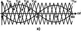 90 180 VollA J360 У 3-v, 30.8-Vj 1 5 9 13 17 21 25 29 33 37 41 45 4в C) f) FIGURE 14.55 Multicell topology. Cell voltages in phase a using a unipolar SPWM (m = 6, = 0.8): (a) Modulating and carrier signals; (b) cell ас output voltage; (c) cell C21 ac output voltage; (d) cell ci ac output voltage; (e) phase a load voltage, (f) phase a load-voltage spectrum. 1 ... 23 24 25 26 27 28 29 ... 91 |
|||||||||||||||||||||||||||||||||||||||||||||||||||||||||||||||||||||||||||||||||||||||||||||||||||||||||||||||||||||||||||||||||||||||||||||||||||||||||||||||||||||||||||||||||||||||||
|
© 2026 AutoElektrix.ru
Частичное копирование материалов разрешено при условии активной ссылки |