 |
 |
 |
| Главная Журналы Популярное Audi - почему их так назвали? Как появилась марка Bmw? Откуда появился Lexus? Достижения и устремления Mercedes-Benz Первые модели Chevrolet Электромобиль Nissan Leaf |
Главная » Журналы » Metal oxide semiconductor 1 ... 24 25 26 27 28 29 30 ... 91 In general, due to the fact that = 3 cells are connected in series in each phase, carriers are required, which should be ф = 360° 7 out of phase. The number of cells per phase depends on the required phase voltage. For instance, a 600-V dc ceU generates an ac voltage of 600 2 = 424 V. Then three cells connected in series generate a phase voltage of 3 424 = 1.27 kV, which in turn generates a 1.27 /3 = 2.2-kV line-to-line voltage. Phases b and с are generated similarly to phase a. Fiowever, the modulating signals i; and v should be 120° out of phase. In order to use identical carrier signals in phases b and c, the carrier-normalized frequency should be a multiple of 3. Thus, three modulating signals and carrier signals are required to generate three phase voltages by means of a multiceU approach, where depends upon the required load hne voltage and the dc bus voltage of each ceU. The ac supply current of each ceU is a six-pulse type of current as shown in Fig. 14.56, which feature harmonics at 6 k± 1 (k = 1,2, ...). Similarly to the load side, the ac supply currents of each ceU are combined so as to achieve high-performance overaU supply currents. Because the front-end converter of each ceU is a six-pulse diode rectifier, a multipulse approach is used. This is based on the natural harmonic canceUation when, for instance, a wye to delta/wye transformer is used to form an iV = 12 pulse configuration from two six-pulse diode rectifiers. In this case, the fifth and seventh harmonics are canceUed out because the supply voltages applied to each six-pulse rectifier become 30° out of phase. In general, to form an N = 6 pulse configuration. set of supply voltages that should be 60°/n out of phase is required. This would ensure the first set of unwanted current harmonics at 6 ± I. The configuration depicted in Fig. 14.54 contains = 9 cells, and a transformer capable of providing = 9 sets of three-phase voltages that should be 60°/n = 60°/9 out of phase to form an N = 6-= 6- 9 = 54-pulse configuration is required. Although this alternative would provide a near-sinusoidal overaU supply current, a fewer number of pulses is also acceptable that would reduce the transformer complexity. An N = 18-pulse configuration usually satisfies aU the requirements. In the example, this configuration can be achieved by means of a transformer with = 9 isolated secondaries; however, only = 3 set of three-phase voltages that are 60°/n = 60°/3 = 20° out of phase are generated (Fig. 14.54). The configuration of the transformer restricts the connection of the ceUs in groups of three as shown in Fig. 14.54. In this case, the fifth, seventh, eleventh, and thirteenth harmonics are canceUed out and thus the first set of harmonics in the supply currents are the seventeenth and the nineteenth. Figure 14.56d shows the resulting supply current that is near-sinusoidal and Fig. 14.56f shows the corresponding spectrum. The fifth, seventh, eleventh, and thirteenth harmonics are stiU there, which is due to the fact that the ac input currents in each ceU are not exactly the six-pulse type of waveforms as seen in Fig. 14.56a,b and c. This is mainly because: (i) the dc link in the ceUs contains a smaU inductor L, which does not smooth out sufficiently the dc bus current (Fig. 14.53a); and (ii) the transformer leakage inductance (or added line induc-
IcQX AdlW 
I it 11 11 I 11 I I I tt I I I I I 11 > ¥ 1 5 9 13 17 21 29 33 37 41 45 49 < (f) overaU current spectrum. tance) smoothes out the edges of the current, which also contributes to the reactive power required by the cells. This last effect is not shown in Fig. 14.56a,b and c. 14.7.2 Multilevel Topologies The six-switch VSI is usually caUed a two-level VSI due to the fact that the inverter phase voltages v, Vy, and v (Fig. 14.52a) are instantaneously either vjl or -vjl. In other words, the phase voltages can take one of two voltage levels. Multilevel topologies provide an alternative to these voltages to take one value out of N levels. For instance. Fig. 14.57 shows an iV = 3-level topology, where the values of the inverter phase voltage are either vJ2, 0, or -vJ2 (Fig. 14.58d). An interesting problem is how to obtain the gating pattern for the 12 switches required in an iV = 3-level topology. There are several modulating techniques to overcome this problem, which can be classified as analog (e.g., carrier-based) and digital (space-vector-based). Both approaches have to deal with the valid switch states of the inverter. 14.7.2.1 Valid Switch States in a Three-Level VSI The easiest way of obtaining the valid switch states is to analyze each phase separately. Phase a contains the switches la ib 4a 4b which cauuot be on simultaneously because a short circuit across the dc bus would be produced, and cannot be off simultaneously because an undefined phase voltage v would be produced. A summary of the valid switch combinations is given in Table 14.7. It is important to note that all vahd switch combinations satisfy the condition that switch state is always the opposite to switch state, and that switch S state is always the opposite to switch S413 state. TABLE 14.7 Valid switch states for a three-level VSI, phase a
Any other switch-state combination would result in an undefined inverter phase a voltage because it wiU depend upon the load-phase current i polarity. The switch states for phases b and с are identical to that of phase a; moreover, because they are paraUeled, they can operate in an independent manner. 14.7.2.2 The SPWM Technique in Three-Level VSIs The main objective is to generate the appropriate 12 gating signals so as to obtain fundamental inverter phase voltages equal to a given set of modulating signals. Specifically, the SPWM in three-level inverters uses a sinusoidal set of modulating signals (v, vy, and v for phases a, b, and c, respectively) and iV - 1 = 2 triangular type of carrier signals {v/i and illustrated in Fig. 14.58a. The best results are obtained if the carrier signals are in-phase and feature an odd normalized frequency = 15. According to Fig. 14.58a, switch is either turned on if v > V/i or off if v < V/i, and switch S is either turned on if v > v2 ca < A2- Additionally, the switch status is obtained as the opposite to switch S, and the switch S status is obtained as the opposite to switch S. In order to use the same set of  FIGURE 14.57 Three-phase three-level VSI topology. Уса Vdl Vcb 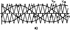 0.8V2 1 3 5 7 9 11 13 15 17 19 21 23 25 27 29 31 4 >61 0.8-0.866-v, 1 3 5 7 9 11 13 15 17 19 21 23 25 27 29 31 0.66v, d) h) FIGURE 14.58 Three-level VSI topology. Relevant waveforms using a SPWM (nif = 15, = 0.8); (a) modulating and carrier signals; (b) switch S status; (c) switch S status; (d) inverter phase a voltage; (e) inverter phase a voltage spectrum; (f) load line voltage; (g) load line voltage spectrum; (h) load phase a voltage. carrier signals to generate the gating signals for phases b and c, the normalized frequency of the carrier signal rUf should be a multiple of 3. Thus, the possible values are trif = 3,9,15,21,.... Figure 14.58 shows the relevant waveforms for a three-level inverter modulated by means of a SPWM technique (m = 15, = 0.8). Specifically, Fig. 14.58d shows the inverter phase voltage, which is clearly a three-level type of voltage, and Fig. 14.58f shows the load line voltage, which shows that the step voltages are at most v/l. More importantly, the inverter phase voltage (Fig. 14.58e) contains harmonics at I rUf ±k with /=1,3,... and = 0,2,4,..., and at I rUf ± к with / = 2, 4, ... and к = 1,3, For instance, the first set of harmonics (/ = 1, = 15) are at 15, 15 ib 2, 15 ib 4, .... The inverter line voltage (Fig. 14.58g) contains harmonics at l-mf±k with /=1,3,... and fc = 2, 4, ..., and at I nij: ±k with / = 2, 4, ... and fc = 1,2, For instance, the first set of harmonics in the line voltages (/ = 1, = 15) are at 15 lb 2, 15 lb 4, .... All the other features of carrier-based PWM techniques also apply in multilevel inverters. For instance: (I) the fundamental component of the inverter phase voltages satisfy am = hm =ст = 1а^ 0 < < 1 (14.88) and thus the line voltages satisfy abl = hcl = cal = а^з|, 0 < < 1 (14.89) where 0 < < 1 is the linear operating region. To further increase the amplitude of the load voltages, the overmodulation operating region can be used by further increasing the modulating signal amplitudes (m > 1), where the line voltages range in. 2 n 2 (14.90) -v,/2 -v,/4 0.8-v,/2 I 11111И1111 I 0.80.866-v, 1 3 1 3 5 1 t I < t I t 7 9 11 13 15 17 19 21 23 25 27 a 31 5 7 9 11 13 15 17 19 21 23 25 27 29 31 FIGURE 14.59 Five-level VSI topology. Relevant waveforms using a SPWM {ruf = 15, = 0.8): (a) inverter phase a voltage; (b) inverter phase a voltage spectrum; (c) load line voltage; (d) load line voltage spectrum. Also: (II) the modulating signals could be improved by adding a third harmonic (zero sequence), which wiU increase the linear region up to = 1.15. This results in a maximum fundamental line-voltage component equal to v. (Ill) a nonsinusoidal set of modulating signals could also be used by the modulating technique. This is the case where nonsinusoidal hne voltages are required as in active filter applications; and (IV) because of the two quadrants operation of VSIs, the multilevel inverter could equally be used in applications where the active power flow goes from the dc to the ac side or from the ac to the dc side. In general, for an iV-level inverter modulated by means of a carrier-based technique, the following conclusions can be drawn: (a) three modulating signals 120° out of phase and N - 1 carrier signals are required; (b) the phase voltages in the inverters have a peak value of v/l; (c) the phase voltages in the inverters are discrete waveforms constructed from the values 2 2 N-Г 2 N-l (14.91) (d) the maximum voltage step in the load voltages is (14.92) for instance, an iV = 5-level inverter requires four carrier signals, the discrete values of the phase voltages are: i;/2, 0, -Vi/4, and -Vi/2, and the maximum step voltage at the load side is Vi/4. Key waveforms are shown in Fig. 14.59. One of the drawbacks of the multilevel inverter is that the dc link capacitors cannot be supplied by a single dc voltage source. This is due to the fact that the currents required by the inverter in the dc bus are not symmetrical and therefore the capacitors wiU not equally share the dc supply voltage v. To overcome this problem, N - 1 independent dc voltage supplies are required. For instance, a three-level inverter will require two supplies that can be constructed by a multipulse transformer; specifically, a wye primary to delta-wye secondaries transformer would fit the requirements. In addition, the supply currents will improve its performance as the fifth and seventh harmonics will be cancelled out. 14.7.2.3 The Space Vector Modulation in Three-Level VSIs Digital techniques are naturally extended to multilevel inverters. In fact, the space vector modulating technique can be applied using the same principles used in two-level inverters. However, the higher number of voltage levels increases the complexity of the practical implementation of the technique. For instance, in iV = 3-level inverters, each leg aUows N = 3 different switch combinations as indicated in Table 14.7. Therefore, there are =27 total valid switch combinations, which generate = 27 load line voltages that are represented by = 27 space vectors (V, V2, ... V27) in Fig. 14.60. For modulating state
43,14 -► a FIGURE 14.60 The space vector representation in a three-level VSI. instance, V2 = 0.5+J0.866 is due to the hne vohages vy = 0.5, Vy = 0.5, v = -1.0 in pu. Thus, although the principle of operation is the same, the space vector digital algorithm wiU have to deal with a higher number of states N. Moreover, because some space vectors (e.g., V13 and Fig. 14.60) produce the same load-voltage terminals, the algorithm wiU have to decide between the two based on additional criteria and that of the basic space vector approach. Clearly, as the number of level increases, the algorithm becomes more and more elaborate. Fiowever, the benefits are not evident as the number of level increases. Five levels is the maximum number used in practical applications. This is based on a compromise between the complexity of the implementation and the benefits of the resulting waveforms. 14.8 Acknowledgments The author is grateful for the financial support from the Chilean Fund for Scientific and Technological Development (FONDECYT) through projects 199 0401 and 799 0071, and from Concepcion University through project P.I. No. 98.092.040-l.In. References Inverters Applications 1. G. Joos and J. Espinoza, Three phase series var compensation based on a voltage controlled current source inverter with supplemental modulation index control, IEEE Trans. Power Electronics 14(3), 587-598 (1999). 2. P. Jain, J. Espinoza, and H. Jin, Performance of a single-stage UPS system for single-phase trapezoidal-shaped ac voltage supplies, IEEE Trans. Power Electronics 13(5), 912-923 (1998). 3. F. Kamran and T. Habetler, A novel on-line UPS with universal filtering capabilities, IEEE Trans. Power Electronics 13(3), 410-418 (1998). 4. H. Akagi, The state-of-the-art of power electronics in Japan, IEEE Trans. Power Electronics 13(2), 345-356 (1998). 5. T. Wu and T. Yu, Off-line applications with single-stage converters, IEEE Trans. Industry Applications 44(5), 638-647 (1997). 6. H. Akagi, New trends in active filters for power conditioning, IEEE Trans. Industry Applications 32(6), 1312-1322 (1996). 7. F. Peng, J. Lai, J. McKeever, and J. van Coevering, A multilevel voltage-source inverter with separate dc sources for static var generation, IEEE Trans. Industry Applications 32(5), 1130-1138 (1996). 8. L. Tolbert, F. Peng, and T. Habetler, Multilevel converters for large electric drives, IEEE Trans. Industry Applicatioins 35(1), 36-44 (1999). 9. J. Espinoza and G. Joos, A current source inverter induction motor drive system with reduced losses, IEEE Trans. Industry Applications 34(4), 796-805 (1998). 10. M. Ryan, W. Brumsickle, and R. Lorenz, Control topology options for single-phase UPS inverters, IEEE Trans Industry Applications 33(2), 493-501 (1997). 11. A. Jungreis and A. Kelly, Adjustable speed drive for residential applications, IEEE Trans. Industry Applications 31(6), 1315-1322 (1995). 12. K. Rajashekara, History of electrical vehicles in General Motors, IEEE Trans. Industry Applicatioins 30(4), 897-904 (1994). 13. B. Bose, Power electronics and motion control - Technology status and recent trends, IEEE Trans. Industry Applications, 29(5), 902-909 (1993). 14. S. Bhowmik and R. Spec, A guide to the application-oriented selection of ac/ac converter topologies, IEEE Trans. Power Electronics, 8(2), 156-163 (1993). 15. B. Wu, S. Dewan, and G. Slemon, PWM -CSI inverter for induction motor drives, IEEE Trans. Industry Applications 28(1), 64-71 (1992). Current Source Inverters 16. F. Antunes, H. Braga, and I. Barbi, Application of a generalized current multilevel cell to current-source inverters, IEEE Trans. Industrial Electronics, 46(1), 31-38 (1999). 17. M. Pande, H. Jin, and G. Joos, Modulated integral control technique for compensating switch delays and nonideal dc buses in voltage-source inverters, IEEE Trans. Industrial Electronics 44(2), 182-190 (1997). 18. J. Espinoza and G. Joos, Current-source converter on-line pattern generator switching frequency minimization, IEEE Trans. Industry Applications 44(2), 198-206, (1997). 19. M. Chandorkar, D. Divan, and R. Lasseter, Control techniques for multiple current source GTO converters, IEEE Trans. Industry Applications 31(1), 134-140 (1995). 20. S. Nonaka and Y. Neba, Current regulated PWM-CSI induction motor drive system without a speed sensor, IEEE Trans. Industry Applications 30(1), 116-125 (1994). 21. G. Joos, G. Moschopoulos, and P. Ziogas, A high performance current source inverter, IEEE Trans. Power Electronics 8:4, 571-579 (1993). 22. C. Hsu and W. Lee, Superconducting magnetic energy storage for power system applications, IEEE Trans. Industry Applications 29P:5, 990-996 (1992). Modulating Techniques and Control Strategies 23. J. Espinoza and G. Joos, DSP implementation of output voltage reconstruction in CSI based converters, IEEE Trans. Industrial Electronics 45(6), 895-904 (1998). 24. M. Kazmierkowski and L. Malesani, Current control techniques for three-phase voltage-source PWM converters: A survey, IEEE Trans. Industrial Electronics 45(5), 691-703 (1998). 25. A. Tilli and A. Tonielli, Sequential design of hysteresis current controller for three-phase inverter, IEEE Trans. Industrial Electronics, 45(5), 771-781 (1998). 26. D. Chung, J. Kim, and S. Sul, Unified voltage modulation technique for real-time three-phase power conversion, IEEE Trans. Industry Applications 34(2), 374-380 (1998). 27. K. Rahman, M. Khan, M. Choudhury, and M. Rahman, Variable-band hysteresis current controllers for PWM voltage-source inverters, IEEE Trans. Power Electronics, 12(6), 964-970 (1997). 28. L. Malesani, P. Mattavelli, and P. Tomasin, Improved constant-frequency hysteresis current control of VSI inverters with simple feed-forward bandwidth prediction IEEE Trans. Industry Applications 33(5), 1194-1202 (1997). 29. M. Rahman, T. Radwin, A. Osheiba, and A. Lashine, Analysis of current controllers for voltage-source inverter, IEEE Trans. Industrial Electronics 477-485 (1997). 30. V. Blasko, Analysis of a hybrid PWM based on modified space-vector and triangle-comparison methods, IEEE Trans. Industry Applications 33(3), 756-764 (1997). 31. Y. Lee, B. Suh, and D. Hyun, A novel PWM scheme for a three-level voltage source inverter with GTO thyristor, IEEE Trans. Industry Applications 32(2), 260-268 (1997). 32. A. Trzynadlowski, R. Kirlin, and S. Legowski, Space vector PWM technique with minimum switching losses and a variable pulse rate, IEEE Trans. Industrial Electronics Щ2), 173-181 (1997). 33. S. Tadakuma, S. Tanaka, H. Naitoh, and K. Shimane, Improvement of robustness of vector-controlled induction motors using feedforward and feedback control, IEEE Trans. Power Electronics 12(2), 221-227 (1997). 34. J. Holtz and B. Beyer, Fast current trajectory tracking control based on synchronous optimal pulse width modulation, IEEE Trans. Industry Applications Ъ\{Ъ), 1110-1120 (1995). 35. A. Trzynadlowski and S. Legowski, Minimum-loss vector PWM strategy for three-phase inverters, IEEE Trans. Power Electronics 9(1) 26-34 (1994). 36. J. Espinoza, G. Joos, and P. Ziogas, Voltage controlled current source inverters, Conf. Rec. IECON9Z San Diego CA, USA, pp. 512-517, November 1992. Overmodulation 37. A. Hava, S. Sul, R. Kerkman, and T. Lipo, Dynamic overmodulation characteristics of triangle intersection PWM methods, IEEE Trans. Industry Applications 35(4), 896-907 (1999). 38. D. Choon and G. Lee, A novel overmodulation technique for space-vector PWM inverters, IEEE Trans. Power Electronics 13(6), 1144-1151 (1998). 39. A. Hava, R. Kerkman, and T. Lipo, Carrier-based PWM-VSI over-modulation strategies: Analysis, comparison, and design, IEEE Trans. Power Electronics 13(4), 674-689 (1998). 40. V. Kaura, A new method to linearize any triangle-comparison-based PWM by reshaping the modulation command, IEEE Trans. Industry Applications 33(5), 1254-1259 (1997). 41. S. Bolognani and M. Zigliotto, Novel digital continuous control of SVM inverters in the overmodulation range, IEEE Trans. Industry Applications 33(2), 525-530 (1997). 42. J. Holtz, W. Lotskat, and A. Khambadkone, On continuous control of PWM inverters in the overmodulation range including the six-step mode, IEEE Trans. Power Electronics 8(4), 546-553 (1993). Selective Harmonic Elimination 43. S. Bowe and S. Grewal, Novel space-vector-based harmonic elimination inverter control, IEEE Trans. Industry Applicationbs 36(2), 549-557 (2000). 44. L. Li, D. Czarkowski, Y. Liu, and P. Pillay, Multilevel selective harmonic elimination PWM technique in series-connected voltage inverters, IEEE Trans. Industry Applications 36(1), 160-170 (2000). 45. J. Espinoza, G. Joos, J. Guzman, L. Moran, and R. Burgos, Selective harmonic elimination and current/voltage control in current/voltage source topologies: A unified approach, Conf. Rec. IECON99, San Jose CA, USA, pp. 318-323, Nov. 29-Dec. 3, 1999. 46. J. Sun, S. Beineke, and H. GrotstoUen, Optimal PWM based on realtime solution of harmonic elimination equations, IEEE Trans. Power Electronics 11(4), 612-621 (1996). 47. H. Karshenas, H. Kojori, and S. Dewan, Generalized techniques of selective harmonic elimination and current control in current source inverters/converters, IEEE Trans. Power Electronics 10(5), 566-573 (1995). 48. H. Patel and R. Hoft, Generalized techniques of harmonic elimination and voltage control in thyristor inverters. Part I-Harmonic elimination, IEEE Trans. Industry Applications IA-9(3), 310-317 (1973). Effects of PWM-Type of Voltage Waveforms 49. N. Aoki, K. Satoh, and A. Nabae, Damping circuit to suppress motor terminal overvoltage and ringing in PWM inveter-fed ac motor drive systems with long motor leads, IEEE Trans. Industry Applications 35(5), 1014-1020 (1999). 50. D. Rendusara and P. Enjeti, An improved inverter output filter configuration reduces common and differential modes dv/dt at the motor terminals in PWM drive systems, IEEE Trans. Power Electronics 13(6), 1135-1143 (1998). 51. S. Chen and T. Lipo, Bearing currents and shaft voltages of an induction motor under hard- and soft-switching inverter excitation, IEEE Trans. Industry Applicatioins 34(5), 1042-1048 (1998). 52. A. von Jouanne, H. Zhang, and A. Wallace, An evaluation of mitigation techniques for bearing currents, EMI and overvoltages in ASD applications, IEEE Trans. Industry Applications 34(5), 1113-1122 (1998). Multilevel Structures 53. L. Tolbert and T. Habetler, Novel multilevel inverter carrier-based PWM method, in IEEE Trans. Industry Applications, 35(5), 1098-1107 (1999). 54. G. Walker and G. Ledwich, Bandwidth considerations for multilevel converters, IEEE Trans. Power Electronics 14(1), 74-81 (1999). 55. Y. Liang and C. Nwankpa, A new type of STATCOM based on cascading voltage-source inverters with phase-shifted unipolar SPWM, IEEE Trans. Industry Applications 35(5), 1118-1123 (1999). 56. N. Schibli, T. Nguyen, and A. Rufer, A three-phase multilevel converter for high-power induction motors, IEEE Trans. Power Electronics 13(5), 978-986 (1998). 57. J. Lai and F. Peng, Multilevel converters - A new breed of power converters, IEEE Trans. Industry Applications 32(3), 509-517 (1997). 58. S. Hal-aacute;sz, A. Hassan, and B. Huu, Optimal control of three-level PWM inverters, IEEE Trans. Industrial Electronics 44(1), 96-106 (1997). 59. R. Menzies, P. Steiner, and J. Steinke, Five-level GTO inverters for large induction motor drives in IEEE Trans. Industry Applications 30(4), 938-944 (1994). 62. B. Ooi, B. Mwinyiwiwa, X. Wang, and G. Joos, Operating limits of the current-regulated delta-modulated current-source PWM rectifier, IEEE Trans. Industrial Electronics 38(4), 268-274 (1991). Regeneration 60. P. Verdelho and G. Marques, DC voltage control and stability analysis of PWM-voltage-type reversible rectifiers, IEEE Trans. Industrial Electronics 45(2), 263-273 (1998). 61. J. Espinoza, G. Joos, and A. Bakhshai, Non-linear control and stabilization of PWM current source rectifiers in the regeneration mode, Conf. Rec. APEC9Z Atlanta GA, USA, pp. 902-908, Feb. 1997. DC Bus Compensation 63. M. Pande, H. Jin, and G. Joos, Modulated integral control technique for compensating switch delays and nonideal dc buses in voltage-source inverters, IEEE Trans. Industrial Electronics 44(2), 182-190 (1997). 64. F. Blaabjerg, J. Pedersen, and P. Thoegersen, Improved modulation techniques for PWM-VSI drives, IEEE Trans. Industrial Electronics 44(1), 87-95 (1997). Resonant and Soft-Switching Converters Prof. S. Y. (Ron) Hui Dr. Henry S. H. Chung Department of Electronic Engineering City University of Hong Kong Tat Chee Avenue, Kowloon, Hong Kong 15.1 Introduction..................................................................................... 271 15.2 Classification.................................................................................... 272 15.3 Resonant Switch............................................................................... 272 15.3.1 ZC Resonant Switch 15.3.2 ZV Resonant Switch 15.4 Quasi-Resonant Converters................................................................. 273 15.4.1 ZCS-QRCs 15.4.2 ZVS-QRC 15.4.3 Comparisons Between ZCS and ZVS 15.5 ZVS in High-Frequency Applications................................................... 275 15.5.1 ZVS with Clamped Vohage 15.5.2 Phase-Shifted Converter with Zero Vohage Transition 15.6 Multiresonant Converters (MRC)........................................................ 280 15.7 Zero-Voltage-Transition (ZVT) Converters............................................ 282 15.8 Nondissipative Active Clamp Network.................................................. 283 15.9 Load Resonant Converters.................................................................. 284 15.9.1 Series Resonant Converters 15.9.2 Parallel Resonant Converters 15.9.3 Series-parallel Resonant Converter 15.10 Control Circuits for Resonant Converters............................................. 287 15.10.1 QRCsandMRCs 15.10.2 Phase-Shifted, ZVT FB Circuit 15.11 Extended-Period Quasi-Resonant (EP-QR) Converters............................ 289 15.11.1 Circuit Operation 15.11.2 Design Procedure 15.12 Soft-Switching and EMI Suppression.................................................... 293 15.13 Snubbers and Soft-Switching for High Power Devices............................. 293 15.14 Soft-Switching DC-AC Power Inverters................................................. 294 15.14.1 Resonant (Pulsating) dc Link Inverter 15.14.2 Active-Clamped Resonant dc Link Inverter 15.14.3 Resonant dc Link Inverter with Low Vohage Stress 15.14.4 Quasi-Resonant Soft-Switched Inverter [47] 15.14.5 Resonant Pole Inverter and Auxihary Resonant Commutated Pole Inverter References........................................................................................ 304 15.1 Introduction Advances in power electronics in the last few decades have led not only to improvements in power devices, but also to new concepts in converter topologies and control. In the 1970s, conventional pulsewidth modulatioin (PWM) power converters were operated in switched mode. Power switches have to cut off the load current within the turn-on and turn-off times under the hard switching conditions. Hard switching refers to the stressful switching behavior of the power electronic devices. The switching trajectory of a hard-switched power device is shown in Fig. 15.1. During the turn-on and turn-off processes, the power device has to withstand high voltage and current simultaneously, which results in high switching losses and stress. Dissipative passive snubbers are usually added to the power circuits so that the dv/dt and di/dt of the power devices can be reduced, and the switching loss and stress can be diverted to the passive snubber circuits. However, switching loss is proportional to switching frequency, thus limiting the maximum switching frequency of the power converters. Typical converter switching frequency was limited to a few tens of kilohertz (typically 20 to 50 kHz) in early 1980s. Stray inductive and capacitive components in the power circuits and power devices stiU cause considerable transient effects, which in turn give rise to electromagnetic interference (EMI) problems. Figure 15.2 shows both typical ideal switching waveforms and practical switching waveforms of the switch voltage. Transient ringing effects are the major cause of EMI. a e eratin Area ard s itc in snubbered т 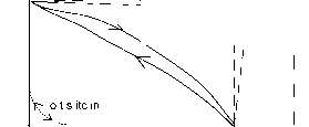 FIGURE 15.1 Typical switching trajectories of power switches. In the 1980s, much research was focused on the use of resonant converters. The concept was to incorporate resonant tanks in the converters to create oscillatory (usually sinusoidal) voltage and/or current waveforms so that zero-voltage switching (ZVS) or zero-current switching (ZCS) conditions could be created for the power switches. Reduction of switching loss and continual improvement of power switches allow the switching frequency of the resonant converters to reach hundreds of kilohertz (typically 100 to 500 kHz). Consequently, the size of magnetic components can be reduced and the power density of the converters increased. Various forms of resonant converters have been proposed and developed. However, most of the resonant converters suffer several problems. When compared with conventional PWM converters, the resonant current and voltage of resonant converters have high peak values, leading to higher conduction loss and higher V and I ratings requirements for the power devices. In addition, many resonant converters require frequency modulation (FM) for output regulation. Variable switching I IDEAL I 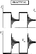 frequency operation makes the filter design and control more complicated. In the late 1980s and throughout the 1990s, further improvements were made in converter technology. New generations of soft-switched converters that combine the advantages of conventional PWM converters and resonant converters were developed. These soft-switched converters have switching waveforms similar to those of conventional PWM converters except that the rising and faUing edges of the waveforms are smoothed with no transient spikes. Unlike the resonant converters, new soft-switched converters usually utilize the resonance in a controlled manner. Resonance is allowed to occur just before and during the turn-on and turn-off processes so as to create ZVS and ZCS conditions. Other than that, they behave just like conventional PWM converters. With simple modifications, many customized control integrated circuits (1С) designed for conventional converters can be employed for soft-switched converters. Because the switching loss and stress have been reduced, soft-switched converters can be operated at the very high frequency (typically 500 kHz to a few megahertz). Soft-switching converters also provide an effective solution to suppress EMI and have been applied to dc-dc, ac-dc and dc-ac converters. This chapter covers the basic technology of resonant and soft-switching converters. Various forms of soft-switching techniques such as ZVS, ZCS, voltage clamping, zero-voltage transition methods etc. are addressed. The emphasis is placed on the basic operating principle and practicality of the converters with only a smaU amount of mathematical analysis. 15.2 Classification This diagram provides at a glance the various types of converters available: Resonant Type DC-DC Converters
phase siiifl-modiilated Constant Frequency Operation Load-Resonant Converters Constant Frequency Operation
15.3 Resonant Switch FIGURE 15.2 Typical ideal and practical switching waveforms. Prior to the availability of fully controUable power switches, thyristors were the major power devices used in power electronic circuits. Each thyristor requires a commutation 1 ... 24 25 26 27 28 29 30 ... 91 |
||||||||||||||||||||||||||||||||||||||||||||||||||||||||||||||||||||||||||||||||||||||||||||||||||||||||||||||||||||||||||||||||||||||
|
© 2026 AutoElektrix.ru
Частичное копирование материалов разрешено при условии активной ссылки |