 |
 |
 |
| Главная Журналы Популярное Audi - почему их так назвали? Как появилась марка Bmw? Откуда появился Lexus? Достижения и устремления Mercedes-Benz Первые модели Chevrolet Электромобиль Nissan Leaf |
Главная » Журналы » Metal oxide semiconductor 1 ... 25 26 27 28 29 30 31 ... 91 (a) (b) FIGURE 15.3 Two types of zero-current (ZC) resonant switch. circuit, which usually consists of an LC resonant circuit, for forcing the current to zero in the turn-off process [1]. This mechanism is in fact a type of zero-current turn-off process. With recent advancements in semiconductor technology, the voltage and current handling capability and the switching speed of fully controllable switches have improved significantly. In many high-power applications, controUable switches such as GTOs and IGBTs have replaced thyristors [2, 3]. Fiowever, the use of a resonant circuit for achieving zero-current-switching (ZCS) and/or zero-voltage-switching (ZVS) [4-8] has also emerged as a new technology for power converters. The concept of resonant switch to replace a conventional power switch is introduced in this section. A resonant switch is a subcircuit composed of a semiconductor switch S and resonant elements and [9-11]. Switch S can be implemented by a unidirectional or bidirectional switch, which determines the operation mode of the resonant switch. Two types of resonant switches [12], including zero-current (ZC) resonant switch and zero-voltage (ZV) resonant switches, are shown in Fig. 15.3 and Fig. 15.4, respectively. 15.3.1 ZC Resonant Switch In a ZC resonant switch, an inductor is connected in series with a power switch S in order to achieve zero-current-switching (ZCS). If the switch S is a unidirectional switch, the switch current is allowed to resonate in the positive half-cycle only. The resonant switch is said to operate in half-wave mode. If a diode is connected in antiparallel with the unidirectional switch, the switch current can flow in both directions. In this case, the resonant switch can operate in full-wave mode. At turn-on, the switch current wiU rise slowly from zero. It will then osciUate because of the resonance between Ц and C. Finally, the switch can be commutated at the next zero current iCr= 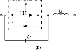 FIGURE 15.4 Two types of zero-voltage (ZV) resonant switch. duration. The objective of this type of switch is to shape the switch current waveform during conduction time in order to create a zero-current condition for the switch to turn off [13]. 15.3.2 ZV Resonant Switch In a ZV resonant switch, a capacitor is connected in paraUel with the switch S for achieving zero-voltage-switching (ZVS). If the switch S is a unidirectional switch, the voltage across the capacitor can osciUate freely in both positive and negative half-cycle. Thus, the resonant switch can operate in full-wave mode. If a diode is connected in antiparallel with the unidirectional switch, the resonant capacitor voltage is clamped by the diode to zero during the negative half-cycle. The resonant switch wiU then operate in half-wave mode. The objective of a ZV switch is to use the resonant circuit to shape the switch voltage waveform during off time in order to create a zero-voltage condition for the switch to turn on [13]. 15.4 Quasi-Resonant Converters Quasi-resonant converters (QRCs) can be considered a hybrid of resonant and PWM converters. The underlying principle is to replace the power switch in PWM converters with the resonant switch. A large family of conventional converter circuits can be transformed into their resonant converter counterparts. The switch current and/or voltage waveforms are forced to osciUate in a quasi-sinusoidal manner, so that ZCS and/or ZVS can be achieved. Both ZCS-QRCs and ZVS-QRCs have half-wave and full-wave modes of operation [8-10, 12]. 15.4.1 ZCS-QRCs A ZCS-QRC designed for half-wave operation is iUustrated with a buck-type dc-dc converter. The schematic is shown in Fig. 15.5a. It is formed by replacing the power switch in a conventional PWM buck converter with the ZC resonant switch in Fig. 15.3a. The circuit waveforms in steady state are shown in Fig. 15.5b. The output filter inductor Ц is sufficiently large so that its current is approximately constant. Prior to turning the switch on, the output current 4 freewheels through the output diode D. The resonant capacitor voltage Vr equals zero. At tg, the switch is turned on with ZCS. A quasi-sinusoidal current /5 flows through Ц and C, the output filter, and the load. Then S is softly commutated at with ZCS again. During and after the gate pulse, the resonant capacitor voltage Vr rises and then decays at a rate depending on the output current. Output voltage regulation is achieved by controUing the switching frequency. Operation and characteristics of the converter depend mainly on the design of the resonant circuit Ц - C. The foUowing parameters are defined: voltage conversion ratio M, characteristic CR1 Lr 1 /rr fr = ate si nal to 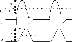 0.9 0.8 0.7 0.6 0.5 0.4 0.3 0.2
FIGURE 15.5 Half-wave, quasi-resonant buck converter with ZCS: (a) Schematic diagram; (b) circuit waveforms; and (c) relationship between M and y. impedance Z, resonant frequency normalized load resistance r, and normalized switching frequency y.  (15.1a) (15.1b) 2vi;:c; (15.1c) (15.1d) (15.1e) It can be seen from the waveforms that if > V/Z, 1 wiU not come back to zero naturally and the switch wiU have to be forced off, thus resulting in turn-off losses. The relationships between M and у at different r are shown in Fig. 15.5c. It can be seen that M is sensitive to the load variation. At light load conditions, the unused energy is stored in C, leading to an increase in the output voltage. Thus, the switching frequency has to be controUed in order to regulate the output voltage. If an antiparaUel diode is connected across the switch, the converter wiU be operating in full-wave mode. The circuit schematic is shown in Fig. 15.6a. The circuit waveforms in steady state are shown in Fig. 15.6b. The operation is simUar to the one in half-wave mode. However, the inductor current is aUowed to reverse through the antiparaUel diode and the duration for the resonant stage is lengthened. This permits excess energy in the resonant circuit at light loads to be transferred back to the voltage source V. This significantly reduces the dependence of on the output load. The relationships between M and у at different r are shown in Fig. 15.6c. It can be seen that M is insensitive to load variation. By replacing the switch in the conventional converters, a family of QRC [9] with ZCS is shown in Fig. 15.7. 15.4.2 ZVS-QRC In these converters, the resonant capacitor provides a zero-voltage condition for the switch to turn on and off. A quasi-resonant buck converter designed for half-wave operation is shown in Fig. 15.8a - using a ZV resonant switch in Fig. 15.4b. The steady-state circuit waveforms are shown in Fig. 15.8b. Basic relations of ZVS-QRCs are given in Eqs. (la)-(le). When the switch S is turned on, it carries output current I. The supply voltage reverse-biases the diode Djr. When the switch is zero-voltage (ZV) turned off, the output current starts to flow through the resonant capacitor C. When the resonant capacitor voltage Vr is equal to Vp turns on. This starts the resonant stage. When V(j equals zero, the antiparaUel diode turns on. The resonant capacitor is shorted and the source voltage is applied to the resonant inductor L. The resonant inductor current 4 increases hnearly untU it reaches I. Then Djr turns off. In order to achieve ZVS, S should be triggered during the time when the antiparaUel diode conducts. It can be seen from the waveforms that the peak amplitude of the resonant capacitor voltage should be greater or equal to the input voltage (i.e., IZ > У^ ). From Fig. 15.8c, 1Г d С :k ate si nal to 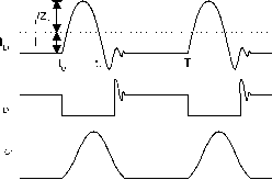 0.9 0.8 0.7 0.6 0.5 0.4 0.3 0.2 0.1
У FIGURE 15.6 Full-wave, quasi-resonant buck converter with ZCS: (a) Schematic diagram; (b) circuit waveforms; and (c)relationship between M and y. it can be seen that the vohage conversion ratio is load-sensitive. In order to regulate the output voltage for different loads r, the switching frequency should also be changed accordingly. Zero-voltage-switching converters can be operated in full-wave mode. The circuit schematic is shown in Fig. 15.9a. The circuit waveforms in steady state are shown in Fig. 15.9b. The operation is similar to half-wave mode of operation, except that yr swing between positive and negative voltages. The relationships between M and у at different r are shown in Fig. 15.9c. By comparing Fig. 15.8c with Fig. 15.9c, it can be seen that M is load-insensitive in full-wave mode. This is a desirable feature. Fiowever, as the series diode limits the direction of the switch current, energy wiU be stored in the output capacitance of the switch and wiU dissipate in the switch during turn-on. Fience, the full-wave mode has the problem of capacitive turn-on loss, and is less practical in high-frequency operation. In practice, ZVS-QRCs are usually operated in half-wave mode rather than full-wave mode. By replacing the ZV resonant switch in the conventional converters, various ZVS-QRCs can be derived. They are shown in Fig. 15.10. 15.4.3 Comparisons Between ZCS and ZVS The ZCS can eliminate the switching losses at turn-off and reduce the switching losses at turn-on. As a relatively large capacitor is connected across the output diode during resonance, the converter operation becomes insensitive to the diodes junction capacitance. When power MOSFETs are zero-current switched on, the energy stored in the devices capacitance wiU be dissipated. This capacitive turn-on loss is proportional to the switching frequency. During turn-on, a considerable rate of change of voltage can be coupled to the gate drive circuit through the MiUer capacitor, thus increasing switching loss and noise. Another hmitation is that the switches are under high-current stress, resulting in higher conduction loss. Fiowever, it should be noted that ZCS is particularly effective in reducing switching loss for power devices (such as IGBT) with large tail current in the turn-off process. The ZVS ehminates the capacitive turn-on loss. It is suitable for high-frequency operation. For single-ended configuration, the switches could suffer from excessive voltage stress, which is proportional to the load. It wiU be shown in Section 15.5 that the maximum voltage across switches in half-bridge and fuU-bridge configurations is clamped to the input voltage. For both ZCS and ZVS, output regulation of the resonant converters can be achieved by variable frequency control. The ZCS operates with constant on-time control, while ZVS operates with constant off-time control. With a wide input and load range, both techniques have to operate with a wide switching frequency range, making it difficult to design resonant converters optimally. 15.5 ZVS in High-Frequency Applications By the nature of the resonant tank and ZCS, the peak switch current in resonant converters is much higher than that in the square-wave counterparts. In addition, a high voltage wiU be established across the switch in the off state after the resonant
  flyback -d= g1=l l1 d13 g1=l f rward -d=
 g1=l FIGURE 15.7 A family of quasi-resonant converters with ZCS. + V - 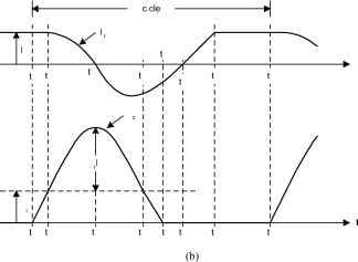 1 cycle 1 0 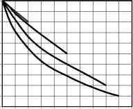 У FIGURE 15.8 Half-wave, quasi-resonant buck converter with ZVS: (a) Schematic diagram; (b) circuit waveforms; and (c) relationship between M and y. Stage. When the switch is switched on again, the energy stored in the output capacitor wiU be discharged through the switch, causing a significant power loss at high frequencies and voltages. This switching loss can be reduced by using ZVS. The ZVS can be viewed as square-wave power utilizing a constant off-time control. Output regulation is achieved by controlhng the on time or switching frequency. During the off time, the resonant tank circuit traverses the voltage across the switch from zero to its peak value and then back to zero again. At that ZV instant, the switch can be reactivated. Apart from
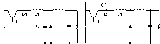
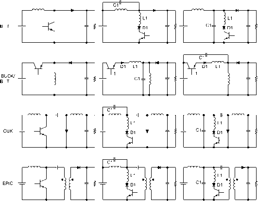
0.9 0.8 0.7 0.6 0.5 0.4 0.3 0.2 0.1 0 0 0.1 0.2 0.3 0.4 0.5 0.6 0.7 0.8 0.9 1 FIGURE 15.9 Full-wave, quasi-resonant buck converter with ZVS: (a) Schematic diagram; (b) circuit waveforms; and (c) relationship between M and y. conventional single-ended converters, some other examples of converters with ZVS are iUustrated in the foUowing section. 15.5.1 ZVS with Clamped Voltage The high-voltage stress problem in the single-switch configuration with ZVS can be avoided in half-bridge (HB) and fuU-bridge (FB) configurations [14]-[17]. The peak switch voltage can be clamped to the dc supply raU, and thus reduces the switch voltage stress. In addition, the series transformer leakage and circuit inductance can form parts of the resonant Buck 6 T Boost о I о Buck boost \ 6 О H Ф I Flyback Ц) 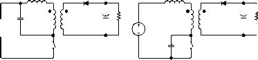 e ic 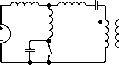 FIGURE 15.10 A family of quasi-resonant converters with ZVS. path. Therefore, these parasitic components, which are undesirable in hard-switched converters, become useful components in ZVS ones. Figures 15.11 and 15.12 show the ZVS HB and FB circuits, respectively, together with the circuit waveforms. The resonant capacitor is equivalent to the parallel connection of the two capacitors (Q/2) across the switches. The off-state voltage of the switches wiU not exceed the input voltage during resonance because they wiU be clamped to the supply rail by the antiparaUel diode of the switches. 15.5.2 Phase-Shifted Converter with Zero Voltage Transition In a conventional FB converter, the two diagonal switch pairs are driven alternatively. The output transformer is fed with an ac rectangular voltage. By applying a phase-shifting approach, a deliberate delay can be introduced between the gate signals to the switches [18]. The circuit waveforms are shown in Fig. 15.13. Two upper or lower switches can be conducting (either through the switch or the antiparaUel diode), yet the applied voltage to the transformer is zero. This zero-voltage condition appears in the interval [1,2] of Vpj-i in Fig. 15.13. This operating stage corresponds to the required off time for that particular switching cycle. When the desired switch is turned off, the primary transformer current flows into the switch output capacitance and this causes the switch voltage to resonate to the opposite input raU. Effects of the parasitic circuit components are used advantageously to facUitate the resonant transitions. This enables a ZVS condition for turning on the opposite switch. Thus, varying the phase shift controls the effective duty cycle and hence the output power. The resonant circuit is necessary to meet the requirement of providing sufficient inductive energy to drive the capacitors to the opposite bus raU. The resonant transition must be achieved within the designed transition time. 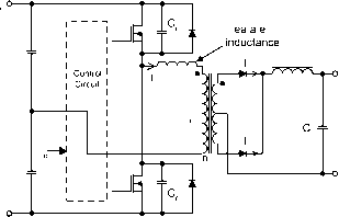 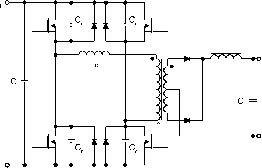 t t t t t t t t 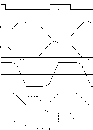 t t t t 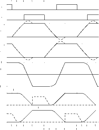 FIGURE 15.11 Half-bridge converter with ZVS. (a) Circuit diagram; FIGURE 15.12 Full-bridge converter with ZVS. (a) Circuit schematic; and (b) circuit waveforms. and (b) circuit waveforms. 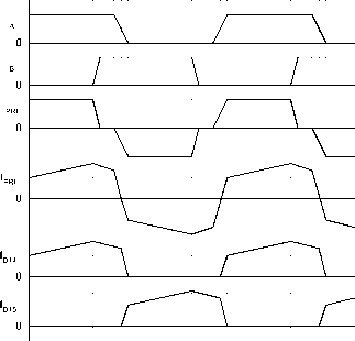 Vl Уз*4 FIGURE 15.13 Circuit waveforms of the phase-shifted, ZVT FB converter. 15.6 Multiresonant Converters (MRC) Both ZCS- and ZVS-QRCs optimize the switching condition for either the active switch or the output diode only, but not for both of them simultaneously. The multiresonant switch concept, which is an extension of the concept of the resonant switch, has been developed to overcome such a limitation. The zero-current multiresonant (ZC-MR) and zero-voltage multiresonant (ZV-MR) switches [12], [17] are shown in Fig. 15.14. The multiresonant circuits incorporate all major parasitic components, including switch output capacitance, diode junction capacitance, and transformer leakage inductance into the resonant circuit. In general, ZVS (half-wave mode) is more favorable than ZCS in dc-dc converters for high-frequency operation because the parasitic capacitance of the active switch and the diode wiU form part of the resonant circuit. An example of a buck ZVS-MRC is shown in Fig. 15.15. Depending on the ratio of the resonant capacitance C/C, two possible topological modes, namely mode I and mode II, can be operated [20]. The ratio affects the time at which the voltages across the switch S and the output diode Df become zero. Their waveforms are shown in Fig. 15.16a, b, respectively. If diode voltage Vj-, faUs to zero earlier than switch voltage V, the converter wiU follow mode I. Otherwise, the converter foUows mode II. Instead of having one resonant stage, there are three in this converter. The mode I operation in Fig. 15.16a is described first. Before the switch S is turned on, the output diode Df is conducting and the resonant inductor current is negative -D d ][ d ][ FIGURE 15.14 MR switch. Multiresonant switches: (a) ZC-MR switch; and (b) ZV- (flowing through the antiparallel diode of S). Then S is then turned on with ZVS. The resonant inductor current I increases linearly and is stiU conducting. When I reaches the output current J, the first resonant stage starts. The resonant circuit is formed by the resonant inductor and the capacitor Cj across the output diode. This stage ends when S is turned off with ZVS. Then, a second resonant stage starts. The resonant circuit consists of L, C, and the capacitor across the switch C. This stage ends when the output diode becomes forward-biased. A third resonant stage wiU then start. Here and form the resonant circuit. This stage ends and completes one operation cycle when the diode becomes forward-biased. The only difference between mode I and mode II in Fig. 15.16b is in the third resonant stage, in which the resonant circuit is formed by Ц and Cj. This stage ends when becomes forward-biased. The concept of the multiresonant switch can be applied to conventional converters [19-21]. A family of MRCs is shown in Fig. 15.17. Although the variation of switching frequency for regulation in MRCs is smaller than that of QRCs, a wide-band frequency modulation is stiU required. Hence, the optimal design of magnetic components and the EMI filters in MRCs is not easy. It would be desirable to have a constant switching frequency operation. In order to operate the MRCs with constant switching frequency, the diode in Fig. 15.14 can be D С : FIGURE 15.15 Buck ZVS-MRC. 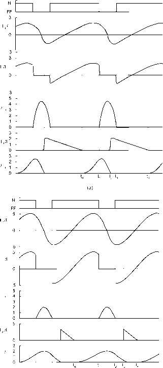 BUCK D =Lc BUCK/B T 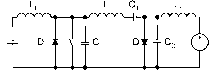 L C, L, ZETA L C, FIGURE 15.16 Possible modes of the buck ZVS-MRC: (a) mode I; and (b) mode II. replaced with an active switch S2 [22]. A constant-frequency multiresonant (CF-MR) switch is shown in Fig. 15.18. The output voltage is regulated by controlling the on-time of the EPIC FIGURE 15.17 Use of the multiresonant switch in conventional PWM converters. two switches. This concept can be illustrated with the buck converter as shown in Fig. 15.19, together with the gate drive waveforms and operating stages. Both Si and s2 are turned on during the time when currents flow through the antiparallel diodes of 5 and S2. This stage ends when S2 is turned off with ZVS. The first resonant stage is then started. The resonant circuit is formed by and q2. A second resonant stage begins. Then Ц resonates with and q2. The voltage across С52Ф \ 2 11-1 FIGURE 15.18 Constant frequency multiresonant switch. Si osciUates to zero. When I becomes negative, wiU be turned on with ZVS. Then resonates with С^2- When current flows through D52 2 wiU be turned on. As the output voltage is the average voltage across s2, output voltage regulation is achieved by controUing the conduction time of s2. All switches in MRCs operate with ZVS, which reduces switching losses and switching noise and ehminates osciUation due to the parasitic effects of the components (such as the Cs1 : 2 , = = Cs2 С j= Rl 1 DRI E WAEF RM 2 DRI E WAEF RM to t. Cs1 L Cs2 [tO,t1] 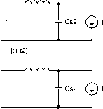 [t2,t3] [t3,t4] FIGURE 15.19 Constant frequency buck MRC: (a) Circuit schematics; (b) gate drive waveforms; and (c) operating stages. junction capacitance of the diodes). However, all switches are under high-current and voltage stresses, resulting in an increase in the conduction loss. 15.7 Zero-Voltage-Transition (ZVT) Converters By introducing a resonant circuit in paraUel with the switches, the converter can achieve ZVS for both power switch and diode without significantly increasing their voltage and current stresses [23]. Figure 15.20a shows a buck-type ZVT- 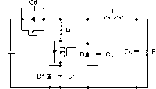 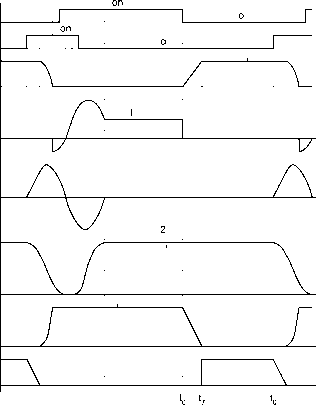 to ti t t, FIGURE 15.20 Buck ZVT-PWM converter: (a) Circuit schematics; and (b) circuit waveforms. 1 ... 25 26 27 28 29 30 31 ... 91 |
|||||||||||||||||||||||||||||||||||||||||||||||||||||||||||||||||||||||||||||||||||||||||||||||||||||||||||||||||||||||||||||||||||||||||||||||||||||||||||||||||||||||||||||||||||||||||||||||||||||||||||||||||||||||||||||||||||||||||||||||||||||||||||||||||||||||||||||||||||||||||||||||||||||||||||||||||||||||||||||||||||||||||||||||||||||||||||||||||||||||||||||||||||||||||||||
|
© 2026 AutoElektrix.ru
Частичное копирование материалов разрешено при условии активной ссылки |