 |
 |
 |
| Главная Журналы Популярное Audi - почему их так назвали? Как появилась марка Bmw? Откуда появился Lexus? Достижения и устремления Mercedes-Benz Первые модели Chevrolet Электромобиль Nissan Leaf |
Главная » Журналы » Metal oxide semiconductor 1 ... 26 27 28 29 30 31 32 ... 91 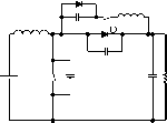 (a) Buck (b) Boost  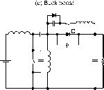 (d) Cuk (e) e ic 0 Zeta FIGURE 15.21 Conventional ZVT-PWM converters. PWM converter and Figure 15.20b shows the associated waveforms. The converter consists of a main switch S and an auxiliary switch S. It can be seen that the voltage and current waveforms of the switches are like squarewave type except during turn-on and turn-off switching intervals, where ZVT takes place. The main switch and the output diode are under ZVS and are subjected to low voltage and current stresses. The auxiliary switch is under ZCS, resulting in low switching loss. The concept of ZVT can be extended to other PWM circuits by adding the resonant circuit. Some basic ZVT-PWM converters are shown in Fig. 15.21. 15.8 Nondissipative Active Clamp Network The active-clamp circuit can utihze the transformer leakage inductance energy and can minimize the turn-off voltage stress in the isolated converters. The active clamp circuit provides a means of achieving ZVS for the power switch and reducing the rate of change of the diodes reverse recovery current. An example of a flyback converter with active clamp is shown in Fig. 15.22a and the circuit waveforms are shown in Fig. 15.22b. Clamping action is obtained by using a series combination of an active switch (i.e., s2) and a large capacitor so that the 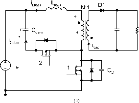 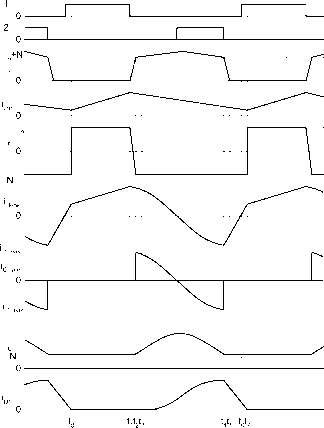 FIGURE 15.22 Active clamp flyback converter: (a) Circuit schematics; and (b) circuit waveforms. voltage across the main switch (i.e., S) is clamped to a minimum value. Then s2 is turned on with ZVS. Fiowever, s2 is turned off with finite voltage and current, and has turn-off switching loss. The clamp-mode ZVS-MRCs is discussed in References [24-26]. 15.9 Load Resonant Converters Load resonant converters (LRCs) have many distinct features over conventional power converters. Due to the soft commutation of the switches, no turn-off loss or stress is present. These LRCs are especially well-suited for high-power applications because they allow high-frequency operation for equipment size/weight reduction, without sacrificing conversion efficiency and imposing extra stress on the switches. Basically, LRCs can be divided into three different configurations, namely series resonant converters, paraUel resonant converters, and series-paraUel resonant converters. 15.9.1 Series Resonant Converters Series resonant converters (SRCs) have their load connected in series with the resonant tank circuit, which is formed by and [15, 27-29]. The half-bridge configuration is shown in Fig. 15.23. When the resonant inductor current is positive, it flows through Tl if is on; otherwise it flows through diode D2. When i is negative, it flows through T2 if T2 is on; otherwise it flows through diode D. In steady-state symmetrical operation, both active switches are operated in a complementary manner. Depending on the ratio between the switching frequency co and the converter resonant frequency ш^, the converter has several possible operating modes. 15.9.1.1 Discontinuous Conduction Mode with CO5 < 0.5co Figure 15.24a shows the waveforms of and the resonant capacitor voltage Vq in this mode of operation. From 0 to t, Tl conducts. From ti to 2, the current in reverses its direction. The current flows through and back to the supply source. From 2 to %, aU switches are in the off state. From Ц to t2 conducts. From 4 to Ц, the current in t2 reverses its direction. The current flows through D2 and back to the supply source. Both and t2 are switched on under ZCS condition and they are switched off under zero current and zero voltage conditions. However, the switches are under 1 cycle 
1 cycle  to t, t3 1 cycle  FIGURE 15.24 Circuit waveforms under different operating conditions: (a) < 0.5(0/, (b) 0.5 < ш^; and (с) < ш^.  7k с FIGURE 15.23 An SRC half-bridge configuration. high current stress in this mode of operation and thus have higher conduction loss. 15.9.1.2 Continuous Conduction Mode with 0.5co < CO5 < co Figure 15.24b shows the circuit waveforms. From 0 to t, transfers from D2 to T. When is switched on with finite switch current and voltage, turn-on switching loss wiU result. Moreover, the diodes must have good reverse recovery characteristics in order to reduce the reverse recovery current. From tl to 2, Dl conducts and is turned off softly with zero voltage and zero current. From 2 to %, t2 is switched on with finite switch current and voltage. At %, t2 is turned off softly and D2 conducts until t. 15.9.1.3 Continuous Conduction Mode with co < co5 Figure 15.24e shows the circuit waveforms. From 0 to t, transfers from to T. Thus, T is switched on with zero current and zero voltage. At t, T is switched off with finite voltage and current, resulting in turn-off switching loss. From to 2, D2 conducts. From 2 to %, t2 is switched on with zero current and zero voltage. At t2 is switched off and transfers from t2 to D. As the switches are turned on with ZVS, lossless snubber capacitors can be added across the switches. The following parameters are defined: voltage conversion ratio M, characteristic impedance Z; resonant frequency normalized load resistance r; and normalized switching frequency 7.
The relationships between M and 7 for different value of r are shown in Fig. 15.25. The boundary between CCM and DCM is at r = 1.277. When the converter is operating in DCM and 0.2 < 7 < 0.5, M= 1.27Г7. 0.9 0.8 0.7 0.6 0.5 0.4 0.3 0.2 0.1 0
The SRC has the following advantages. Transformer saturation can be avoided because the series capacitor can block the dc component. The light load efficiency is high because both device current and conduction loss are low. Fiowever, the major disadvantages are that there is difficulty in regulating the output voltage under light load and no load conditions. Moreover, the output dc filter capacitor has to carry high ripple current, which could be a major problem in low-output voltage and high-output current apphcations [29]. 15.9.2 Parallel Resonant Converters ParaUel resonant converters (PRCs) have their load connected in parallel with the resonant tank capacitor [27-30]. The half-bridge configuration is shown in Fig. 15.26. The SRC behaves as a current source, whereas the PRC acts as a voltage source. For voltage regulation, PRC requires a smaller operating frequency range than the SRC to compensate for load variation. 15.9.2.1 Discontinuous Conduction Mode The steady-state waveforms of the resonant inductor current ii and the resonant capacitor voltage Vq are shown in Fig. 15.27a. Initially both i and Vq are zero. From 0 to 2, T conducts and is turned on with zero current. When i is less than the output current J, increases linearly from 0 to t and the output current circulates through the diode bridge. From to %, Ц resonates with C. Starting from 2, ii reverses its direction and flows through . Then T is turned off with zero current and zero voltage. From t to t, Vq decreases linearly due to the relatively constant value of 4. At when Vq equals zero, the output current circulates through the diode bridge again. Both i and Vq wiU stay at zero for an interval. From t to 9, the preceding operations wiU be repeated for t2 and D2. The output voltage is controUed by adjusting the time interval of [4, 5]. 15.9.2.3 Continuous Conduction Mode co5 < co This mode is simUar to the operation in the DCM, but with a higher switching frequency. Both i and Vq become continuous. The waveforms are shown in Fig. 15.27b. The switches 0.5 0.6 0.7 0.8 0.9 1 У FIGURE 15.25 M vs 7 in SRC.
FIGURE 15.26 The PRC half-bridge configuration. 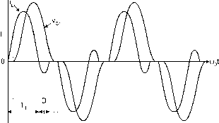
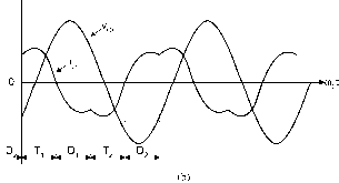
FIGURE 15.27 Circuit waveforms under different operating conditions: (a) Discontinuous conduction mode; (b) continuous conduction mode < ш^; and (с) continuous conduction mode > ш^. and t2 are hard turned on with finite voltage and current and are soft turned off with ZVS. 15.9.2.3 Continuous Conduction Mode co5 > co If the switching frequency is higher than ш^, the antiparallel diode of the switch will be turned on before the switch is triggered. Thus, the switches are turned on with ZVS. However, the switches are hard turned off with finite current and voltage. FIGURE 15.28 M vs у in PRC. shown in Fig. 15.28. During the DCM (i.e., 7 < 0.5), M is in linear relationship with 7. Output voltage regulation can be achieved easily. The output voltage is independent of the output current. The converter shows good voltage source characteristics. It is also possible to step up and step down the input voltage. n:1 re
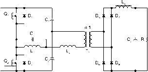 The parameters defined in Eq. (15.2) are apphcable. The FIGURE 15.29 Different types of SPRC: (a) LCC-type; and (b) LLC-relationships between M and 7 for various values of r are type. The PRC has the advantages that the load can be short-circuited and the circuit is suitable for low-output voltage, high-output current applications. However, the major disadvantage of the PRC is the high device current. Moreover, as device current does not decrease with the load, the efficiency drops with a decrease in the load [29]. 15.9.3 Series-Parallel Resonant Converter The series-paraUel resonant converter (SPRC) combines the advantages of the SRC and the PRC. The SPRC has an additional capacitor or inductor connected in the resonant tank circuit [29-31]. Figure 15.29a shows an LCC-type SPRC, in which an additional capacitor is placed in series with the resonant inductor. Figure 15.29b shows an LLC-type SPRC, in which an additional inductor is connected in parallel with the resonant capacitor in the SRC. Fiowever, there are many possible combinations of the resonant tank circuit. Detailed analysis can be found in Reference [31]. 15.10 Control Circuits for Resonant Converters Since 1985s, various control integrated circuits (ICs) for resonant converters have been developed. Some common ICs for different converters are described in this section. 15.10.1 QRCsandMRCs Output regulations in many resonant-type converters, such as QRCs and MRCs, are achieved by controUing the switching frequency. The ZCS apphcations require controlled switch-on times whUe ZVS applications require controUed switch-off times. The fundamental control blocks in the 1С include an error amphfier, voltage-controUed-osciUator (VCO), one-shot generator with a zero wave-crossing detection comparator, and an output stage to drive the active switch. Typical ICs include UC1861-UC1864 for ZVS applications and UC 1865-UC 1868 for ZCS applications [32]. Figure 15.30 shows the controller block diagram of UC 1864. The maximum and minimum switching frequencies (i.e., .in) controUed by the resistors Rge min capacitor C ; / and f can be expressed as (Knge/min)Q< and f = Rmin VCO (15.3) The frequency range А/ is then equal to A/ fmsix fmin Range YCO (15.4) The frequency range of the ICs is from 10 kFiz to 1 MFiz. The output frequency of the oscillator is controUed by the error amplifier (E/A) output. An example of a ZVS-MR forward converter is shown in Figure 15.31. 15.10.2 Phase-Shifted, ZVT FB Circuit The UCC3895 is a phase-shift FWM controUer that can generate a phase shifting pattern of one half-bridge with respect to the other. The application diagram is shown in Fig. 15.32. The four outputs OUTA, OUTB, OUTC, and OUTD are used to drive the MOSFETs in the fuU-bridge. The dead time between OUTA and OUTB is controlled by DELAB and the dead time between OUTC and OUTD is controUed by
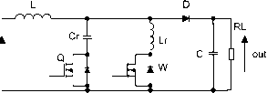
0.5V  Fault Logic and Precision Reference BiasSc 5V Gen UVLO
-CD Gnd НГП Vcc -o 0Ш A -a Out В -I i Pwr Gnd FIGURE 15.30 Controller block diagram of UC1864 (Courtesy of Unitrode Corp. and Texas Instruments, www.ti.com). 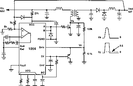 FIGURE 15.31 The ZVS-MR forward converter (Courtesy of Unitrode Corp. and Texas Instruments, www.ti.com). RT[i] CT[ I I I SYNC [б]-I RAMP Цу. . 8(rt) EAOUT EAP EAN PWM COMPARATOR ERROR AMP I 2V О CS [H CURRENT SENSE COMPARATOR OVER CURRENT j-jMPARAT0R D S Q N0 LOAD COMPARATOR 0.5V/ 0.6V О 10( rt) D S 0 R -> -ЛЛЛг- ADAPTIVE DELAY SET AMPLIFIER -wv- UVLO COMPARATOR ±1 0.5V ЛЛЛгО DISABLE COMPARATOR 0.5V o-i- -О 11V/9V REFERENCE OK COMPARATOR -+1-0 4V в 7] DELAB OUTB OUTC DELCD ill lel PGND ADS FIGURE 15.32 Application diagram of UCC3895 (Courtesy of Unitrode Corp. and Texas Instruments, www.ti.com). DELCD. Separate delays are provided for the two half-bridges to accommodate differences in resonant capacitor charging currents. The delay in each set is approximated by delay - 25 x IQ-idel 0.75(Vcs - W + 0.5 + 25ns (15.5) where iel is the resistor value connected between DELAB or DELCD to ground. The osciUator period is determined by Rj and Cj. It is defined as fesc=+120 ns (15.6) The maximum operating frequency is 1 MHz. The phase shift between the two sets of signals is controUed by the ramp voltage and an error amplifier output with a 7 MHz bandwidth. 15.11 Extended-Period Quasi-Resonant (EP-QR) Converters Generally, resonant and quasi-resonant converters operate with frequency control. The extended-period quasi-resonant converters proposed by Barbi [33] offer a simple solution to modify existing hard-switched converters into soft-switched ones with constant frequency operation. This makes both output filter design and control simple. Figure 15.33 shows a standard hard-switched boost-type PFC converter. In this hard-switched circuit, the main switch SWl could be subject to significant switching stress because the reverse recovery current of the diode Dp could be excessive when SWl is turned on. In practice, a smaU saturable inductor may be added in series with the power diode Dp in order to reduce the di/dt of the reverse-recovery current. In addition, an optional R-C snubber may be added across SWl to reduce the dv/dt of SWl. These extra reactance components can, in fact, be used in the EP-QR circuit to achieve soft switching, as shown in Fig. 15.34. The resonant components Ц and have smaU values and can come from the snubber circuits of a standard hard-switched converter. Thus, the only additional component is the auxUiary switch Q2. The smaU resonant inductor is put in series with the main switch SWl so that SWl can be switched on under ZC condition and the di/dt problem of the reverse-recovery current be ehminated. The resonant capacitor is 1 ase ACsu ly 1 ase ACsu ly FIGURE 15.34 The EP-QR boost-type ac-dc power factor correction circuit. used to Store energy in order to create the condition for soft switching. The Q2 is used to control the resonance during the main switch transition. It should be noted that aU power devices including SWl, Q, and main power diode D are turned on and off under ZV and/or ZC conditions. Therefore, the large di/dt problem due to the reverse recovery of the power diode can be eliminated. The soft-switching method is an effective technique for EMI suppression. Together with the power factor correction technique, softswitching converters offer a complete solution to meet EMI regulations for both conducted and radiated EMI. The operation of the EP-QR boost PFC circuit [34, 35] can be described in six modes (a-f) as shown in Fig. 15.35. The corresponding idealized waveforms are included in Fig. 15.36. 15.11.1 Circuit Operation Interval I: (to-ti). Due to the resonant inductor L, which limits the di/dt of the switch current, switch SW is turned on at zero-current condition with a positive gating signal Vq to start a switching cycle at t = t. Current in Dp is diverted to inductor L. Because Dp is stiU conducting during this short 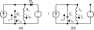 62 r l С l
О FIGURE 15.33 Boost-type ac-dc power factor correction circuit. FIGURE 15.35 Operating modes of EP-QR boost-type ac-dc power factor correction circuit. 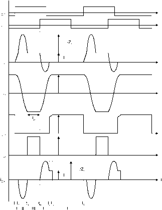 FIGURE 15.36 Idealized waveforms of EP-QR boost-type ac-dc power factor correction circuit. diode of SW. This current is limited by Ц and thus Q2 is turned on under a zero-current condition. Because the anti-parallel diode of SW is conducting, the voltage across SWl is clamped to the on-state voltage of the antiparaUel diode. Therefore SW can be turned off at (near) zero-voltage condition before t = 2, at which the second half of the resonant cycle ends. Interval V: (t - h). During this interval, the voltage across Q is less than the output voltage V. Therefore, Dp is stiU reverse-biased. Inductor current flows into Q untU V reaches at t = Ц. The equivalent circuit is represented in Fig. 15.35e. Interval VI: (ts-tj). During this period, the resonant circuit is not in action and the inductor current /5 charges the output capacitor Cp via Dp, as in the case of a classical boost-type PFC circuit. The is charged to and Q2 can be turned off at zero-voltage and zero-current conditions. Figure 15.35f shows the equivalent topology of this operating mode. In summary, SWl, Q2 and Dp are fully soft-switched. Because the two resonance half-cycles take place within a closed loop outside the main inductor, the high resonant pulse wiU not occur in the inductor current, thus making the weU-established averaged current mode control technique apphcable for such a QR circuit. For fuU soft-switching in the turn-off process, the resonant components need to be designed so that the peak resonant current exceeds the maximum value of the inductor current. Typical measured switching waveforms and trajectories of SWl, Q2 and Dp are shown in Fig. 15.37, Fig. 15.38, and Fig. 15.39, respectively. period, D52 is stiU reversed biased and is thus not conducting. The equivalent circuit topology for the conducting paths is shown in Fig. 15.35a. Resonant switch Q2 remains off in this interval. Interval II: (ti -1), When Dp regains its blocking state, D52 becomes forward biased. The first half of the resonance cycle occurs and resonant capacitor starts to discharge and current flows in the loop C-Q2-L;.-SWi. The resonance half-cycle stops at time t = because D52 prevents the loop current from flowing in the opposition direction. The voltage across is reversed at the end of this interval. The equivalent circuit is shown in Fig. 15.35b. Interval III: (t- tb). Between and t, current in Lp and continues to buUd up. This interval is the extended period for the resonance during which energy is pumped into L. The corresponding equivalent circuit is showed in Fig. 15.35c. Interval IV: (tb-z)- Figure 15.35d shows the equivalent circuit for this operating mode. Before SW is turned off, the second half of the resonant cycle needs to take place in order that a zero-voltage condition can be created for the turn-off process of SWj. The second half of the resonant cycle starts when auxUiary switch Q2 is turned on at t = t. Resonant current then flows through the loop L-Q2-Q-antiparaUel 15.11.2 Design Procedure Given: Input ac voltage = . Peak AC vohage V, (V) Nominal output dc voltage = V(V) Switching frequency = /5 (Hz) Output power = Po(W) Input current ripple = A/(A) Output voltage ripple = AV(V) 15.11.2.1 Resonant Tank Design Step 1: Because the peak resonant current must be greater than the peak inductor current (same as peak input line current) in order to achieve soft-turn-off, it is necessary to determine the peak input current s(max) Assuming lossless ac-dc power conversion, /(max) Ьс estimated from the foUowing equation: 2V / 00 s(max) (15.7) s(max) where 1 = Pglo the maximum output current. IBKUMfl 12MS/$ 111 Acgs Ш UU.UU VDC 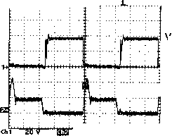 4 ISW lOOmV 2)15 124mV ТвкЕЩВ 12SMS/S I25MS/S 19 Acq: ,?;7;т:Тиг;Т;уУ77м';;;т;г.л 1Э Acqs 00.00 VDC S: iHMlm.j.  124mV (a) (b) FIGURE 15.37 (a) Drain-source voltage and current of SWl; and (b) switching locus of SWl. ТёкшШШ 12SMS/S 436 Acqs CS 00.00 VDC 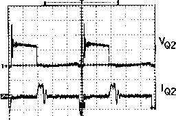 Chi 20 0 lOOmv 2its a2> -84mv ТэкСШБ 125MS/S 18 Acqs ES3 00.00 VDC 18 AtS Ш 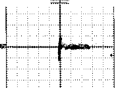 Chi 20 у ВЙ idomv tii2> -84mv (a) (b) FIGURE 15.38 (a) Drain-source voltage and current of Q2; and (b) switching locus of Q2. ItekRun: 12SMS/$ sample гттт-гттгД^ут-гтттт 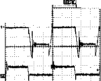 S 00.00 VDC 56mv ДеКЦШВ 125MS/S 163 Acqs LSI) UU.UU VDC 56mV (a) (b) FIGURE 15.39 (a) Diode voltage and current; and (b) switching locus of diode. Step 2: Soft-switching criterion is (15.8) s(max) where = .LJC is the impedance of the resonant tank. For a chosen resonant frequency and Q can be obtained from 271/, = i/yi;c; 15.11.2.2 Filter Component Design The minimum conversion ratio is (15.9) (min in) ~ o/s(max) №w r+ Vsw) (15.10) 1Г 5. Hui and H. Chung L
 where T = 1 and is the extended period. From Eq. (5.10), minimum can be estimated. The turn-on period of the SWl is on(swl) - + V/?- Inductor value i is obtained from (15.11) on(swl) d 4<- Го 5 f / s(max) The filter capacitor value С can be determined from С T,/sin Ч4/)у (15 12) FIGURE 15.40 A family of EP-QR converters: (a) Buck converter; (b) boost converter; and (c) flyback converter. (15.13) where = 1 is the period of the ac voltage supply frequency. LOG REF 130.0 cJBijV 10 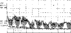 START 9.0 kHz STOP 30.00 MHz #IF BW 9.0 kHz AVG BW 30 kHz SWP 1.11 sec REF 90.0 dBpV ATTEN 10 d PEAK LOG 10 dB/
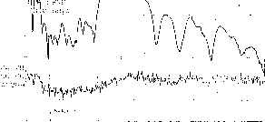 START 30.0 MHz #RES BW 120 kHz STOP 300.0 MHz VBW 300 kHz SWP 5Б msec (a) (b) FIGURE 15.41 (a) Conducted EMI from hard-switched flyback converter; and (b) radiated EMI from hard-switched flyback converter. 1 ... 26 27 28 29 30 31 32 ... 91 |
|||||||||||||||||||||||||||||||||||||||||||||||||||||||||||||||||||||||||||||||||||||||||||||||||||||||||||||||||||||||||||||||||||||||||||||||||||||||||||||||||||||||||||||||||||||||||||||||||||||||||||||||||||||||||||||||||||||||||||||||||||||||||||||||||||||||||||||||||||||||||||||||||||||||||||||||||||||||||||||||||||||||||||||||||||||||||
|
© 2026 AutoElektrix.ru
Частичное копирование материалов разрешено при условии активной ссылки |