 |
 |
 |
| Главная Журналы Популярное Audi - почему их так назвали? Как появилась марка Bmw? Откуда появился Lexus? Достижения и устремления Mercedes-Benz Первые модели Chevrolet Электромобиль Nissan Leaf |
Главная » Журналы » Metal oxide semiconductor 1 ... 27 28 29 30 31 32 33 ... 91 LOG REF 130.0 cJBijV 10 dB/ #ATN 50 dB 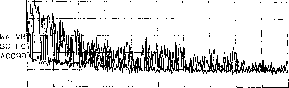 START 9.0 kHz STOP 30.00 MHz #IF BW 9.0 kHz AVG BW 30 kHz SWP 1.11 sec REF 90. 0 clBpV ATTEN 10 dB PEAK 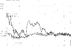 START 30.0 MHz STOP 300.0 MHz #RES BW 120 kHz VBW 300 kHz SWP 56 msec FIGURE 15.42 (a) Conducted EMI from soft-switched flyback converter; and (b) radiated EMI from soft-switched flyback converter. 15.12. Soft-Switching and EMI Suppression A family of EP-QR converters is displayed in Fig. 15.40. Their radiated EMI emission have been compared with that from their hard-switched counterparts [36]. Figure 15.41a, b shows the conducted EMI emission from a hard-switched flyback converter and a soft-switched one, respectively. Their radiated EMI emissions are included in Fig. 15.42. Both converters are tested at an output power of 50W. No special filtering or shielding measures have been taken during the measurement. It is clear from the measurements that soft-switching is an effective means to EMI suppression. 15.13 Snubbers and Soft-Switching for High Power Devices Today, most of the medium power (up to 200 kVA) and medium voltage (up to 800 V) inverters are hard-switched. Compared with low-power switched mode power supplies, the high voltage involved in the power inverters makes the dv/dt, di/dt, and switching stress problems more serious. In addition, the reverse recovery of power diodes in the inverter leg may cause a very sharp current spike, leading to severe EMI problems. It should be noted that some high-power devices such as GTO thyristors do not have a square safe operating area (SOA). It is therefore essential that the switching stress they undergo must be within their limits. Commonly used protective measures include the use of snubber circuits to protect high-power devices. Among various snubbers, two snubber circuits are most well known for apphcations in power inverters. They are the Undeland snubber [37] (Fig. 15.43) and McMurray snubber circuits [38] (Fig. 15.44). The Undeland snubber is an asym- metric snubber circuit with one turn-on inductor and one turn-off capacitor. The turn-off snubber capacitor is clamped by another capacitor C. At the end of each switching cycle, the snubber energy is dumped into and then discharged into the dc bus via a discharge resistor. In order to reduce the snubber loss, the discharge resistor can be replaced by a switched mode circuit. In this way, the Undeland snubber can become a snubber with energy recovery. The McMurray snubber is symmetrical. Both of the turn-off cdc=r undeland FIGURE 15.43 Undeland snubber. cs/2 4= ls/2 : cdc4= D i- ls/2: cs/2 4= mcmurray FIGURE 15.44 McMurray snubber. 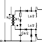 Cdc4= i-° FIGURE 15.45 McMurray snubber with energy recovery. snubber capacitors share current in parallel during turn off. The voltage transient is limited by the capacitor closest to the turning-off device because the stray inductance to the other capacitor will prevent instantaneous current sharing. The turn-on inductors require midpoint connection. Snubber energy is dissipated into the snubber resistor. Like the Undeland snubber, the McMurray snubber can be modified into an energy recovery snubber. By using an energy recovery transformer as shown in Fig. 15.45. this snubber becomes a regenerative one. Although other regenerative circuits have been proposed, their complexity makes them unattractive in industrial applications. In addition, they do not necessarily solve the power diode reverse recovery problems. Although the use of snubber circuits can reduce switching stress in power devices, the switching loss is actually damped into the snubber resistors unless regenerative snubbers are used. The switching loss is stiU a limiting factor to the high frequency operation of power inverters. However, the advent of soft-switching techniques opens up a new way to use high-frequency inverter operation. Because the switching trajectory of a soft-switched switch is close to the voltage and current axis, faster power electronic devices with smaller SOAs can, in principle, be used. In general, both ZVS and ZCS can reduce switching loss in high-power power switches. However, for power switches with tail currents, such as IGBT, ZCS is more effective than ZVS. 15.14 Soft-Switching DC-AC Power Inverters The soft-switching technique not only offers a reduction in switching loss and thermal requirement, but also aUows the possibility of high frequency and snubberless operation. Improved circuit performance and efficiency as weU as reduction of EMI emission can be achieved. For zero voltage switching (ZVS) inverter applications, two major approaches that enable inverters to be soft-switched have been proposed. The first approach puUs the dc link voltage to zero momentarily so that the inverters switches can be turned on and off with ZVS. Resonant dc link and quasi-resonant inverters belong to this category. The second approach uses the reso- nant pole idea. By incorporating the filter components into the inverter operation, resonance condition and thus zero voltage/current conditions can be created for the inverter switches. In this section, the following soft-switched inverters are described. Approach A: Resonant dc link inverters: 1. resonant (pulsating) dc link inverters; 2. actively-clamped resonant dc link inverters; 3. resonant inverters with minimum voltage stress; 4. quasi-resonant soft-switched inverter; and 5. parallel resonant dc link inverter. Approach B: Resonant pole inverters: 6. resonant pole inverters; 7. auxiliary resonant pole inverters; and 8. auxiliary resonant commutated pole inverters. Type 1 is the resonant dc link inverter [39-41], which sets the dc hnk voltage into osciUation so that zero-voltage instants are created periodically for ZVS. Despite the potential advantages that this soft-switching approach can offer, a recent review on existing resonant link topologies for inverters [42] concludes that the resonant dc link system results in an increase in circuit complexity and the frequency spectrum is restricted by the need to use integral pulse density modulation (IPDM) when compared with a standard hard-switched inverter. In addition, the peak pulsating link voltage of resonant link inverters is twice that of the dc link voltage in a standard hard-switched inverter. Although clamp circuits (Type 2) can be used to limit the peak voltage to 1.3-1.5 per unit [41], power devices with higher than normal voltage ratings have to be used. Circuits of Types 3-5 employ a switched mode front stage circuit, which puUs the dc link voltage to zero momentarily whenever inverter switching is required. This soft-switching approach does not cause extra voltage stress to the inverter and hence the voltage rating of the power devices is only 1 per unit. As ZVS conditions can be created at any time, there is virtually no restriction in the PWM strategies. Therefore, weU-established PWM schemes developed in the last two decades can be employed. In some ways, this approach is similar to some dc-side commutation techniques proposed in the past for thyristor inverters [43, 44], although these dc-side commutation techniques were used for turning off thyristors in the inverter bridge and not primarily developed for soft-switching. Circuits of Types 6-8 retain the use of a constant dc link voltage. They incorporate the use of the resonant components and/or filter components into the inverter circuit operation. This approach is particularly useful for inverter applications in which output filters are required. Examples include uninterruptible power supplies (UPS) and inverters with output filters for motor drives. The LC filter components can form the auxiliary resonant circuits that create the soft-switching conditions. However, these tend to have high-power device count and require complex control strategy. 15.14.1 Resonant (Pulsating) dc link inverter A resonant dc link converter for dc-ac power conversion was proposed in 1986 [39]. Instead of using a nominally constant dc link voltage, a resonant circuit is added to cause the dc link voltage to pulsate at a high frequency. This resonant circuit theoretically creates periodic zero-voltage duration at which the inverter switches can be turned on or off. Figure 15.46 shows the schematics of the pulsating link inverter. Typical dc link voltage, inverters phase voltage, and the line voltages are shown in Fig. 15.47. Because the inverter switching can only occur at zero voltage duration, integral pulse density modulation (IPDM) has to be adopted in the switching strategy. Analysis of the resonant dc hnk converter can be simplified by considering that the inverter system is highly inductive. The equivalent circuit is shown in Fig. 15.48. The link current 4 У ith the changing load condition, but can be considered constant during the short resonant cycle. If switch S is turned on when the inductor current is 4о' the resonant dc link voltage can be expressed as 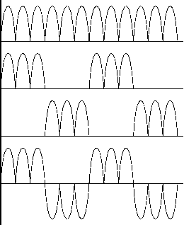 V(t) = V, + e-l-V cos(cot) + coLIm sm(cot)] (15.14) FIGURE 15.47 Typical dc link voltage (Fq), phase voltages {V, F), and line voltage of resonant link inverters.     FIGURE 15.48 Equivalent circuit of resonant link inverter. and inductor current ip is
4f - ho ~ 4 (15.19) The resistance in the inductor could affect resonant behavior because it dissipates some energy. In practice, {ip - IJ has to be monitored when S is conducting. In addition, S can be turned on when (i - IJ is equal to a desired value. The objective is to ensure that the dc link voltage can be resonated to zero voltage level in the next cycle. The pulsating dc link inverter has the foUowing advantages: reduction of switching loss; snubberless operation; high switching frequency (> 18 kHz) operation becomes possible, leading to the reduction of acoustic noise in inverter equipment; and reduction of heat sink requirements and thus improvement of power density. This approach has the foUowing limitations: The peak dc pulsating link voltage (2.0 per unit) is higher than the nominal dc voltage value of a conventional inverter. This implies that power devices and circuit components of higher voltage ratings must be used. This could be a serious drawback because power components of higher voltage ratings are not only more expensive, but usually have inferior switching performance than their low-voltage counterparts. Although voltage clamp can be used to reduce the peak dc link voltage, the peak voltage value is stiU higher than normal and the additional clamping circuit makes the control more complicated. Integral pulse-density modulation has to be used. Many weU-established PWM techniques cannot be employed. Despite these advantages, this resonant converter concept has paved the way for other soft-switched converters to develop. 15.14.2 Active-Clamped Resonant dc Link Inverter In order to solve the high-voltage requirement in the basic pulsating dc link inverters, active clamping techniques (Fig. 15.49) have been proposed. The active clamp can reduce the per-unit peak voltage from 2.0 to 1.3 - 1.5 [41]. It has been reported that an operating frequency in the range of 60 to 100 kHz has been achieved [45] with an energy efficiency of 97% for a 50-kVA drive system. The design equations for an active-clamped resonant link inverter are Tl = - = 2l;c;\ cos 4l - ) + k-l i (15.20) where is the minimum link period, fi is the maximum link frequency, and к is the clamping ratio. For the active-clamped resonant inverter, к is typically 1.3 to 1.4 p.u. The rate of rise of the current in the clamping device is di (k-l)V, dt~ и (15.21) The peak clamping current required to ensure that the dc bus return to zero voltage is  k{2 - k)C (15.22) 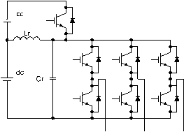 In summary, resonant (pulsating) dc link inverters offer significant advantages, such as: high switching frequency operation; low (ii;/(it for power devices; ZVS with reduced switching loss; suitable for l-250kW; and rugged operation with few failure modes. 15.14.3 Resonant dc Link Inverter with Low Voltage Stress A resonant dc hnk inverter with low voltage stress [46] is shown in Fig. 15.50. It consists of a front-end resonant converter that can puU the dc link voltage down just before any inverter switching. This resonant dc circuit serves as an interface between the dc power supply and the inverter. It essentially retains aU the advantages of the resonant (pulsating) dc link inverters but it offers extra advantages, including: No increase in the dc link voltage when compared with a conventional hard-switched inverter. That is, the dc link voltage is 1.0 per unit. The zero voltage condition can be created at any time. The ZVS is not restricted to the periodic zero-voltage instants as in a resonant dc link inverter. WeU-estabhshed PWM techniques can be employed. Power devices of standard voltage ratings can be used. The timing program and the six operating modes (a-f) of this resonant circuit are as shown in Fig. 15.51 and Fig. 15.52, respectively. (1) Normal mode This is the standard PWM inverter mode. The resonant inductor current ZlfCO the resonant voltage vcr(0 are given by iu(t) = 0 VcXt) = V, where is the nominal dc link voltage. (2) Mode 1 (Initiating mode): (tQ - tJ At tg, mode 1 begins by switching T2 and T3 on with zero current. Then ZlfCO increases hnearly with a di/dt of VJL. If zlrco is equal to the 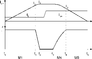 M2 M3 FIGURE 15.51 Timing diagram of a resonant link inverter with minimum voltage stress. initialized current Tl is zero-voltage turned off. If (/ - 4) < /p then the initialization is ended when ZlfCO is equal to where I is the current flowing into the dc inductor Lj. If (/ - IJ > then this mode continues until ZlfCO is equal to (/ - 4). The equations in this interval are (3) Mode 2 (Resonant mode): (ti - t2) After Tl is turned off under the ZVS condition, resonance between and Q occurs. The VXO decreases from to 0. At iu(t) reaches the peak value in this interval. The equations are 4г(0 = sin(a;,t) + [Ji + (4 - Q] cos(co,t) - (I, - Q VJt) -V, cos(co,0 - [I, + (I, - Q]Z, sm(co,t) kih) = h = 4г,реак Vh) = 0 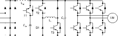 where 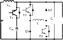 == mi do + © (a) normal mode (b) mode 1 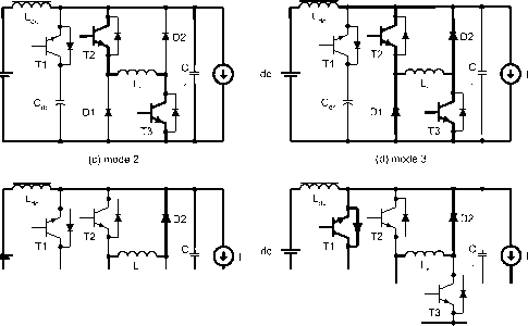  (e) mode 4 () mode 5 FIGURE 15.52 Operating modes of resonant link inverter with minimum voltage stress. = J-f and (4) Mode 3 (Freewheeling mode): (t2 - Ц) The resonant inductor current flows through two freewheehng paths (T2-Lr-D2 and T3-Dl-Lr). This duration is the zero voltage period created for ZVS of the inverter, and should be longer than the minimum on and off times of the inverters power switches: Ш = h (5) Mode 4 (Resonant mode): - tJ This mode begins when T2 and T3 are switched off under ZVS. The second half of the resonance between and Q starts again. The capacitor voltage Vcr(t) increases back from 0 to and is clamped to V. The relevant equations in this mode are Ш = [I2 - (Ion - Q] COs(CD,t) - - /,) V,Xt) = [l2-(Ion-Is)]ZrSm(co,t) kritd = h where I is the load current after the switching state. (6) Mode 5 (Discharging mode): (t - Ц) In this period, Tl is switched on under ZV condition because Vcr(0 = s- The inductor current decreases linearly. This mode finishes when iirit) becomes zero. kAh) = 0 15.14.4 Quasi-Resonant Soft-Switched Inverter [47] 15.14.4.1 Circuit Operation Consider an inverter fed by a dc voltage source V. A front-stage interface circuit shown in Fig. 15.53 can be added between the dc voltage source and the inverter. The front stage circuit consists of a quasi-resonant circuit in which the first half of the resonance cycle is set to occur to create the zero-voltage condition whenever inverter switching is needed. After inverter switching has been completed, the second half of the resonance cycle takes place so that the dc link voltage is set back to its normal level. To avoid excessive losses in the resonant circuit, a smaU capacitor Ci is normally used to provide the dc hnk voltage while the large smoothing dc link capacitor is isolated from the resonant circuit just before the zero-voltage duration. This method avoids the requirement for pulling the dc voltage of the bulk capacitor to zero. The period for this mode is from t to in Fig. 15.54. In this mode, switch is turned on and switches S and S2 turned off. The inverter in Fig. 15.53 works like a conventional dc link inverter and Vri = this mode. The voltage across switch is zero. Before an inverter switching takes place, switch Si is triggered at to discharge C. This operating mode ends at 2 when V approaches zero. The equivalent circuit in this mode is shown in Fig. 15.55a. The switch must be turned off at zero voltage when switch Si is triggered. After S is triggered, C wiU be discharged via the loop Ci, C2 ri- Under conditions of У^2 - Ql < Q2 energy stored in Ci wiU be transferred to C2 Vj-i faUs to zero in the first half of the resonant cycle in the equivalent circuit of Fig. 15.55a. Vri be clamped to zero by the freewheel diodes in the inverter bridge and wiU not become negative. Thus, V can be pulled down to zero for zero voltage switching. When the current in inductor becomes zero, switch S can be turned off at zero current. Inverter switching can take place in the period from 2 to t in which Vj-i remains zero. This period must be longer than the turn-on and turn-off times of the switches. When inverter switching has been completed, it is necessary to reset the voltage of capacitor C The equivalent circuit in this mode is shown in Fig. 15.55b. The current in inductor reaches zero at %. Due to the voltage in V2 the presence of diode D, 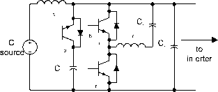 I °
FIGURE 15.54 Typical waveforms for Vi and ¥2- this current then flows in the opposite direction. Then Ci wiU be recharged via 4, C2 Qi Diode turns off when the current in Ц becomes zero. Fiere Vri beyond 1 per unit because C is clamped to supply voltage by diode D. Switch can be turned on again at zero voltage condition when Vi returns to normal dc supply voltage. After Dr turns /\ l  (a) Mode (b) Mode 4 FIGURE 15.53 Quasi-resonant circuit for soft-switched inverter. (c) Mode 5 FIGURE 15.55 Equivalent circuits of the quasi-resonant circuit for different modes. off, Vy2 be zero. Some positive residual capacitor voltage remains in c2 at t, as shown in Fig. 15.54. In the case Kr2 is positive, V cannot be pulled down to zero again in the next switching cycle. Therefore, S2 should be triggered after 4 to reverse the residual vohage in C2- time 82 turns off at zero current condition and V2 is now reversed to negative. The equivalent circuit in this mode is shown in Fig. where 15.55c. When V2 < 0 and Qi < q2, Vn can be pulled down to zero again before the next inverter switching. The operation can then be repeated in next switching cycle. should be turned on a half-resonant cycle before the inverter switching instant. The turn-on instant of S, which is in Fig. 15.54, can be written as CD = ,2-2 a = (15.25) 15.14.4.2 Design Considerations: (1) and q2 The criterion for getting zero capacitor vohages yri (Ql - C,2)Vs + 2C,2Vo2 - А/ 7ifL;C, < 0 (15.23) where Vi is the initial voltage of Q; V2 is the initial voltage of iiQ is the initial current of inductor L/, А/ = - /5, which is the difference between load current and supply current. It is assumed to be a constant within a resonant cycle; is the equivalent resistance in the resonant circuit; and q1q2 Ql + Q: When А/ > 0, the preceding criterion is always true under conditions of: Ql < q2, V02 < 0 The criterion for recharging voltage V-i to 1 per unit dc link voltage is: Ql + q2 V02- Ql + q2 (15.24) (2) Inductor Ц The Ц should be smaU so that the dc link voltage can be decreased to zero quickly. However, a smaU Ц could result in large peak resonant current and therefore requirement of power devices with large current pulse ratings. An increase in the inductance of can limit the peak current in the quasi-resonant circuit. Because the resonant frequency depends on both the inductor and the capacitor, the selection of Ц can be considered together with capacitors Qi and q2 and with other factors such as the current ratings of power devices, the zero-voltage duration, and the switching frequency required in the soft-switching circuit. (3) Triggering instants of the switches Correct triggering instants for the switches are essential for the successful operation of this soft-switched inverter. For inverter switches, the triggering instants are determined from a PWM modulation. Let be the time at which the inverter switches change states. To get the zero voltage inverter switching, switch Si The switch is turned off at t. The Si may be turned off during its zero current period when diode is conducting. For easy implementation, its turn-off time can be selected as + я/ш. Because the dc link voltage can be pulled down to zero in less than half of a resonant cycle, should occur between 2 and At time 3 (the exact instant depends on the A/), the diode turns on in the second half of the resonant cycle to recharge Ql. At Vj-i reaches 1 per unit and diode clamps V-i to 1 per unit. The switch can be turned on again at t, which is a half resonant cycle after the start of %: (15.26) As % cannot be determined accurately, a voltage sensor can be used, in principle, can be used to provide information for t so that Si, can be turned on to reconnect Q to the inverter. In practice, however, can be turned on a few microseconds (longer than Ts + я/ш) after 2 without using a voltage sensor (because it is not critical for to be on exactly at the moment Vj. reaches the nominal voltage). As for switch S2 it can be turned on a few microseconds after t. It wiU be turned off half of resonant cycle {п^[ЦС~2) in the - q2 circuit later. In practice, the timing of Si, 82 and can be adjusted in a simple tuning procedure for a given set of parameters. Figure тек ШШ 5MS/S 21 Acqs [ T ] I Sb Sr2 * Vcrl Ш2 IV 10)1$ FIGURE 15.56 Gatings signals for S, S,2 and with 15 Resonant and Soft-Switching Conveners rekmiSB2MS/s 2097 Acqs Vcrl \ 46f W и'Ш Ш'У (a lOmV 25>iS FIGURE 15.57 Typical 4, 4 d Vi under no-load condition. 15.56 shows the measured gating signals of S, S2 ih the dc link voltage V in a 20-kFiz switching inverter. Figures 15.57 and 15.58 show typical 4, and I under no-load and loaded conditions, respectively. 15.14.4.3 Control of Quasi-Resonant Soft-Switched Inverter using Digital Time Control Based on the zero-average-current error (ZACE) control concept, a digital time control (DTC) method [48] has been developed for a current-controlled quasi-resonant soft-switched inverter. The basic ZACE concept is shown in Fig. 15.59. The current error is obtained from the difference of a reference current and the sensed current. The idea is to have the areas of each transition (Al and A2) equal. If the switching Гак 2MS/S 25 Acqs [ T  romv 25ms FIGURE 15.58 Typical 4 and F.i under loaded condition. error current, A
*n *n+ *n+ *n+3 *n+4 *n+5 FIGURE 15.59 Zero-average-current error (ZACE) control concept. л digital signal processor A - 8 interrupt switch control reference sine wa e QRC delay comparator current error turn-on delay sensed Iq output turn-on delay FIGURE 15.60 Implementation of DTC. 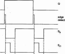 \J i across FIGURE 15.61 Timing diagrams for the gating signals. i-f-Г \-\-...... \...... 4........  FIGURE 15.62 (a) Typical switch voltage under hard turn-off; and (b) typical switch voltage under soft-turn-off.
Load FIGURE 15.63 One leg of a resonant pole inverter. - =r C1 L=Lr С =r C2 - =h C3 D4t - =H C4 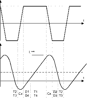 FIGURE 15.64 Single-phase resonant pole inverter. frequency is significantly greater than the fundamental frequency of the reference signal, the rising and faUing current segments can be assumed to be hnear. The following simplified timing diagram for a single-phase resonant pole inver-equation can be established: Cx=C1,C2,C3,C4=Cr/2 ter. (15.27) T1 ± T4 ± Lr=L l=lr + о
+ о T2 ± T3 ±
+ 0 +0 FIGURE 15.66 Operating mode of a single-phase resonant pole inverter. 1 ... 27 28 29 30 31 32 33 ... 91 |
||||||||||||||||||||||||||||||||||||||||||||||||||||||||||||||||||||||||||||||||||||||||||
|
© 2026 AutoElektrix.ru
Частичное копирование материалов разрешено при условии активной ссылки |