 |
 |
 |
| Главная Журналы Популярное Audi - почему их так назвали? Как появилась марка Bmw? Откуда появился Lexus? Достижения и устремления Mercedes-Benz Первые модели Chevrolet Электромобиль Nissan Leaf |
Главная » Журналы » Metal oxide semiconductor 1 ... 38 39 40 41 42 43 44 ... 91 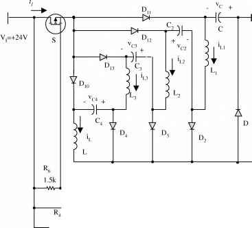 820 -Wv-
Ro R. 1.5k X 510 3.9k FIGURE 17.73 The 1000-V insulation test bench  TABLE 17.11 The measured experimental results
 The intervals are: . V,{h + h)f V, cos \ ....... Average output voltage v2 and input current are: FIGURE 17.74 The MIT 42/14-V 3-kW dc/dc converter. TABLE 17.12 Experimental results for different frequency
 FIGURE 17.75 The IBM 1.8-V/200-A power supply. I -fc The power transfer efficiency is When we set = 180 V and frequency / = 200-250 kHz, we obtained v2 = 1-8 V, N= 12, Iq = 0-200 A, Volume = 14 (in). The average power-transfer efficiency is 94% and the maximum power density (PD) is 25.7 W/in. References 1. Luo, F. L., Double Output Luo-Converters, An Advanced Voltage Lift Technique. IFF Proc. Electric Power Applications 147: (6), 469-485, November 2000. 2. Luo, F. L., Positive Output Luo-Converters, Voltage Lift Technique. IFF Proc. Electric Power Applications 146: (4), 415-432, July 1999. 3. Luo, F. L., Negative Output Luo-Converters, Voltage Lift Technique. IFF Proc. Electric Power Applications 146: (2), 208-224, July 1999. 4. Luo, F. L., Re-Lift Converter: Design, Test, Simulation and Stability Analysis. IFF Proc. Electric Power Applications 145: (4), 315-325, July 1998. 5. Rashid, M. H., Power Electronics: Circuits, Devices and Applications, 2nd ed., Prentice-Hall, Englewood Cliffs, 1993. 6. Mohan, N., Undeland, T. M., and Robbins, W. P., Power Electronics: Converters, Applications and Design, John Wiley & Sons, New York, 1995. 7. Severns, R. P. and Bloom, G. Modern DC-to-DC Switchmode Power Converter Circuits, Van Nostrand Reinhold Company, New York, 1985. 8. Kularatna, N. Power Electronics Design Handbook, John Wiley & Sons, New York, 1985. 9. Luo, F. L. Neural Network Control for Synchronous Rectifier DC/DC Converter, Proceedings of the International Conference ICARCY2000, Singapore, 5-8 December 2000 (CD ROM). 10. Luo, R L., Ye, H., and Rashid, M. H., Two-Quadrant DC/DC ZCS Quasi-Resonant Luo-Converter, Proceedings of the IEEE International Conference IPEMC2000, Beijing, China, August 15-18, 2000, pp. 272-277. 11. Luo, R L., Ye, H., and Rashid, M. H., Two-Quadrant DC/DC ZVS Quasi-Resonant Luo-Converter, Proceedings of the IEEE International Conference IPEMC/2000, Beijing, China, August 15-18, 2000, pp. 1132-1137. 12. Luo, F. L. Negative Output Luo-Converters - Voltage Lift Technique, Proceedings of the Second World Energy System International Conference WES98, Toronto, Canada, May 19-22, 1998, pp. 253-260. 13. Luo, F. L., Ye, H., and Rashid, M. H., Four-Quadrant Operating Luo-Converters, Proceedings of the IEEE International Conference PESC2000, Galway, Ireland, 18-23 June 2000, pp. 1047-1052. 14. Luo, F. L., 42/14 V Two-Quadrant DC/DC soft-switching Converter, Proceedings of the IEEE International Conference PESC2000, Galway, Ireland, 18-23 June 2000, pp. 173-178. 15. Luo, F. L. and Ye, H., Two-Quadrant Switched Capacitor Converter, Proceedings of the 13th Chinese Power Supply Society IAS Annual Meeting, Shenzhen, China, 15-18 November 1999, pp. 164-168. 16. Luo, F. L. and Ye, H., Four-Quadrant Switched Capacitor Converter, Proceedings of the 13th Chinese Power Supply Society IAS Annual Meeting Shenzhen, China, 15-18 November 1999, pp. 513-518. 17. Luo, F. L., Ye, H., and Rashid, M. H., Switched Capacitor Four-Quadrant Luo-Converter Proceedings of the IEEE - IAS Annual Meeting, IAS99, Phoenix, Arizona, USA, 3-7 October 1999, pp. 1653-1660. 18. Luo, F. L., Ye, H., and Rashid, M. H., Switched Inductor Four-Quadrant Luo-Converter, Proceedings of the IEEE - IAS Annual Meeting IAS99, Phoenix, Arizona, USA, 3-7 October 1999, pp. 1631-1638. 19. Luo, F. L., Four-Quadrant DC/DC ZCS Quasi-Resonant Luo-Converter, Accepted for publication by lEE International Conference IPEC2001, Singapore, 17-19 May 2001. 20. Gao, Y. and Luo, F. L., Theoretical Analysis on Performance of a 5 V/12 V Push-pull Switched Capacitor DC/DC Converter, Accepted for publication by lEE International Conference IPEC2001, Singapore, 17-19 May 2001. 21. Luo, F. L. and Chua, L. M., Fuzzy Logic Control for Synchronous Rectifier DC/DC Converter, Proceedings of the lASTED International Conference ASC2000, Banff, Alberta, Canada, July 24-26, 2000, pp. 24-28. 22. Luo, F. L., Luo-Converters - Voltage Lift Technique, Proceedings of the IEEE Power Electronics Special Conference IEEE-PESC98, Fukuoka, Japan, May 17-22, 1998, pp. 1783-1789. 23. Luo, F. L., Luo-Converters, A Series of New DC-DC Step-Up (Boost) Conversion Circuits, Proceedings of the IEEE International Conference PEDS97, 26-29 May 1997, Singapore, pp. 882-888. 24. Luo, F. L., Re-Lift Circuit, A New DC-DC Step-Up (Boost) Converter. lEE-Electronics Letters 33: (1), 5-7, Jan. 1997. 25. Luo, F. L., Lee, W. C, and Lee, G. В., Self-Lift Circuit, A New DC-DC Converter, Proceedings of the 3rd National Undergraduate Research Programme (NURP), Congress 97, Singapore, 13th Sept. 1997, pp. 31-36. 26. Luo, F. L., DSP-Controlled PWM L-Converter Used for PM DC Motor Drives, Proceedings of the IEEE International Conference SISCTA97, Singapore, 29-30 July 1997, pp. 98-102. 27. Luo, F. L., Luo-Converters, New DC-DC Step-Up Converters, Proceedings of the lEE International Conference ISIC-97, 10-12 September 1997, Singapore, pp. 227-230. 28. Smedley, K. M. and Cuk, S. Dynamics of One-Cycle Controlled Cuk Converter. IEEE J. Quantum Electron. Trans. PE 10: (6) 617-639, November 1995. 29. Smedley, K. M. and Cuk, S., One-Cycle Control of Switching Converters. IEEE Trans. PE 10: (6), 625-633, November 1995. 30. Maksimovic, D. and Cuk, S., Switching Converters with Wide DC Conversion Range. IEEE J. Quantum Electron. Trans. PE 6: (1), 151-157, January 1991. 31. Maksimovic, D. and Cuk, S., A General Approach to Synthesis and Analysis of Quasi-Resonant Converters. IEEE Trans. PE 6: (1) 127-140, Jan. 1991. 32. Maksimovic, D. and Cuk, S., Constant-Frequency Control of Quasi-Resonant Converters. IEEE Trans. PE 6: 91), 141-150, January 1991. 33. Middlebrook, R. D. and Cuk, S., Advances in Switched-Mode Power Conversion, Vols. I and II, TESLAco, Pasadena, CA, 1981. 34. Liu, Y. and Sen, P. C, New Class-E DC-DC Converter Topologies with Constant Switching Frequency. lEEE-IA Transactions 32: (4), 961-969, July/August 1996. 35. Redl, R., Molnar, В., and Sokal, N. O., Class-E Resonant DC-DC Power Converters: Analysis of Operations, and Experimental Results at 1.5 MHz. IEEE Trans., Power Electronics, 1: 111-119, April 1986. 36. Kazimierczuk, M. K. and Bui, X. Т., Class-E DC-DC Converters with an Inductive Impedance Inverter. IEEE Trans., Power Electronics 4: 124-135, July 1989. 37. Massey, R. R and Snyder, E. C, High Voltage Single-Ended DC-DC Converter. IEEE PESQ 1977 Record, pp. 156-159. 38. Jozwik, J. J. and Kazimerczuk, M. K., Dual Sepic PWM Switching-Mode DC/DC Power Converter. IEEE Trans. Industrial Electronics 36: (1), 64-70, 1989. 39. Martins, D. C, Application of the Zeta Converter in Switch-Mode Power Supplies, Proc. of IEEE APEC93, USA, pp. 214-220. 40. Kassakian, J. G., Wolf, H-C, Miller, J. M., and Hurton, C. J., Automotive electrical systems, circa 2005, IEEE Spectrum, August 1996, pp. 22-27. 41. Wang, J., Dunford, W. G., and Mauch, K., Some Novel Four-Quadrant DC-DC Converters. Proc. IEEE-PESC9S, Fukuoka, Japan, pp. 1775-1782. 42. Luo, F. L., Double Output Luo-Converters, Proceedings of the lEE International Conference IPEC99, Singapore, 24-26 May 1999, pp. 647-652. 43. Ye, H. and Luo, F. L., Luo-Converters, A Series of New DC-DC Step-Up Conversion Circuits. International Journal < Power Supply Technologies and Applications > 1: (1), April 1998, Xian, China, pp. 30-39. 44. Ye, H. and Luo, F. L., Advanced Voltage Lift Technique - Negative Output Luo-Converters. International Journal < Power Supply Technologies and Applications > 1: (3 , August 1998, Xian, China, pp. 152-168. 45. Luo, F. L., Negative Output Luo-Converters - Voltage Lift Technique, Proceedings of the Second World Energy System International Conference WES98, Toronto, Canada, May 19-22, 1998, pp. 253-260. 46. Luo, F. L., Luo-Converters - Voltage Lift Technique, Proceedings of the IEEE Power Electronics Special Conference IEEE-PESC98, Fukuoka, Japan, May 17-22, 1998, pp. 1783-1789. 47. Luo, F. L. and Ye, H., Two-Quadrant DC/DC Converter with Switched Capacitors, Proceedings of the International Conference IPEC99, Singapore, 24-26 May 1999, pp. 641-646. 48. Midgley, D. and Sigger, M., Switched-capacitors in power control. lEE Proc. 121: 703-704, July 1974. 49. Cheong, S. V., Chung, H., and loinovici. A., Inductorless DC-DC Converter with High Power Density. IEEE Trans. Industrial Electronics 41: (2), 208-215, April 1994. 50. Midgley, D. and Sigger, M., Switched-capacitors in power control. lEE Proc. Ill: 703-704, July 1974. 51. Chung, H., Hui, S. Y. R., and Tang, S. C, A low-profile switched-capacitor-based DC/DC converter. Proc. AUPEC97, Oct. 1997, pp. 73-78. 52. Ngo, K. D. T. and Webster, R., Steady-state analysis and design of a switched-capacitor DC-DC converter. IEEE Trans. ANES 30: (1), 92-101, January 1994. 53. Harris, W. S. and Ngo, K. D. Т., Power Switched-capacitor DC-DC converter: analysis and design. IEEE Trans. ANES 33: (2), 386-395, April 1997. 54. Tse, C. K., Wong, S. C, and Chow, M. H. L., On lossless switched-capacitor power converters. IEEE Trans. PE 10: (3), 286-291, May 1995. 55. Мак, О. С, Wong, Y. С, and loinovici. A., Step-up DC power supply based on a switched-capacitor circuit. IEEE Trans. IE 42: (1), 90-97, February 1995. 56. Мак, О. С. and loinovici, A. Switched-capacitor inverter with high power density and enhanced regulation capability. IEEE Trans. CAS-7 45: (4), 336-347, April 1998. 57. Luo, F. L. and Ye, H., Switched Inductor Two-Quadrant DC/DC Converter with Fuzzy Logic Control, Proceedings of IEEE International Conference PEDS99, Hong Kong, 26-29 July 1999, pp. 773-778. 58. Luo, F. L. and Ye, H., Switched Inductor Two-Quadrant DC/DC Converter with Neural Network Control, Proceedings of IEEE International Conference PEDS99, Hong Kong, 26-29 July 1999, pp. 1114-1119. 59. Liu, K. H. and Lee, F. C, Resonant Switches - A Unified Approach to Improved Performances of Switching Converters, International Telecommunications Energy Conference (INTELEC) Proc, Nov. 4-7, 1984, New Orleans, LA, USA, pp. 344-351. 60. Liu, K. H. and Lee, F. C, Zero-Voltage Switching Techniques in DC/DC Converter Circuits, Power Electronics Specialists Conf. (PESO) Record, June 1986, Vancouver, Canada, pp. 58, 70. 61. Martinez, Z. R. and Ray, В., Bidirectional DC/DC Power Conversion Using Constant-Frequency Multi-Resonant Topology, Applied Power Electronics Conf. (APEC) Proc, Feb. 13-17, 1994, Orlando, FL, USA, pp. 991-997. 62. Pong, M. H., Ho, W. C, and Poon, N. K., Soft switching converter with power limiting feature. lEE-EPA Proceedings 146: (1), 95-102, January 1999. 63. Gu, W. J. and Harada, K., A novel self-excited forward DC-DC converter with zero-voltage-switched resonant transitions using a saturable core. lEEE-PE Transactions 10: (2), 131-141, March 1995. 64. Cho, J. G., Sabate, J. A., Hua, G., and Lee, F. C, Zero-voltage and zero-current-switching full bridge PWM converter for high power applications. lEEE-PE Transactions 11: (4), 622-628. July 1996. 65. Poon, N. K. and Pong, M. H., Computer aided design of a crossing current resonant converter (XCRC), Proceedings of IECON9i Bologna, Italy, 5-9 Sept. 1994, pp. 135-140. 66. Kassakian, J. G., Schlecht, M. R, and Verghese, G. C, Principles of Power Electronics, Addison-Wesley, New York, 1991, p. 217. Gate Drive Circuits M. Syed J. Asghar, Ph.D. Department of Electrical Engineering Aligarh Muslim University Aligarh, India 18.1 18.2 18.3 18.4 18.5 18.6 Introduction...................................................................................... 407 Thyristor Gate Requirements................................................................ 407 Trigger Circuits for Thyristors.............................................................. 409 Simple Gate Trigger Circuits for Thyristors............................................. 410 18.4.1 Resistance Trigger Circuits 18.4.2 RC Trigger Circuits 18.4.3 Diac Trigger Circuit 18.4.4 AC-Thyratron Type Trigger Circuit 18.4.5 Unijunction Transistor-Based Trigger Circuit 18.4.6 Advanced Triggering Circuits for Thyristors 18.4.7 Buffer and Driver Circuits for Thyristors Drivers for Gate Communication Switches............................................. 422 18.5.1 Gate Drive Circuits for Power MOSFETs 18.5.2 Design Consideration of MOSFET Driver Circuits 18.5.3 Driver Circuits for IGBT 18.5.4 Transistor-Based Drive Circuits 18.5.5 Gate Drive Circuit for GTO Some Practical Driver Circuits.............................................................. 427 References.......................................................................................... 429 18.1 Introduction A gate signal is required for every power semiconductor-controlled device to bring it into the conduction state. Fiowever, the nature of the gate drive requirement (or the base drive requirement for power bipolar junction transistor (BJT) and Darlington power transistor) of each device varies, depending on the voltage and current rating and also on the type of the device (i.e., thyristors or gate-commutation devices). The gate drive requirements of thyristors (sihcon controlled rectifier, SCR), Triac, etc. are different from the gate drive requirements of the gate-commutation devices, viz. gate-turn-off thyristor (GTO), power BJT, metal-oxide field effect transistor (MOSFET), insulated-gate bipolar transistor (IGBT), static induction transistor (SIT), MOS-controUed thyristor (MCT), and so forth. Therefore, gate drive circuits of thyristors and gate-commutation devices are discussed here separately. 18.2 Thyristor Gate Requirements A thyristor can be triggered by the apphcation of a positive gate voltage {Vq) and hence a gate current {Iq) supplied from a gate drive circuit as shown in Fig. 18.1. Fiowever, the choice of Vq and Iq is not restricted to a particular value, rather it varies over a wide range. It depends on the gate characteristics of the device as shown in Fig. 18.2. Any operating point {Vq, Iq) may be selected within the permissible or preferred gate drive area bounded by curves 1, 2, 3, 4, 5, and the rectangle mnop. Curve 3 represents a constant value of the maximum permissible gate power dissipation Р^м- Moreover, there is a nontrigger gate voltage {Vqj)), which is a minimum gate voltage below which a thyristor cannot be triggered at any temperature (normally up to 100 °C). This gives a permissible noise level of the gate drive circuit that will not trigger the thyristor. The rectangle mnop is prescribed by the manufacturers to avoid both unsuccessful and undesirable triggering in the worst cases. It corresponds to the threshold condition of triggering {Vqj, Iqt)- Also, it is related to forward anode voltage {Vjj) and junction temperature {Ту). For lower temperature, Vqj and Iqj increase and therefore the size of the rectangle mnop increases. Similarly, it should be ensured that the gate-circuit load-line {wxyz) should pass above this area. Fiowever, the most preferred zone for the operating point is close to curve 3. This, in turn, increases the di/dt capability, minimizes the switching-on time, and hence reduces the switching loss of the thyristor. Gate trigger circuits can be designed with the help of both Figs. 18.1 and 18.2. Curve 6 shows the gate-to-cathode forward v-i characteristics of the device at given V and T. This is the same as the forward-conducting characteristics of a silicon diode. The load-line wxyz of the gate trigger circuit intersects the device characteristics at q. Thus operating gate voltage {Vq) and gate current {Iq) are given by or and os respectively. The permissible range of the operating point is between x and y. The maximum or short-circuit current of the trigger source is Е^/{Щ-\- Р^), which is shown by ow; 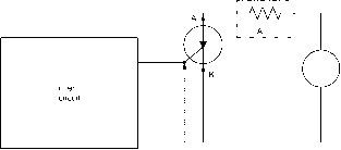 Also, A Г  Л/Vv-  n er source figure 18.1 A typical switching arrangement for an SCR. 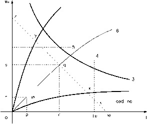 figure 18.2 Typical gate characteristics of an SCR. should be selected such that this current is not harmful to the source as weU as to the gate-to-cathode junction (/3). Similarly, oz shows the maximum trigger source voltage Eg. The presence of R2 is optional, however, if Eg is greater than VM it helps to clip Vq not to exceed the У^м ll otherwise /3 may be damaged. Moreover, R2 provides a low gate-to-cathode impedance in the off-state of the device, thus improving the thyristor noise immunity. When R2 is connected across G and К terminals, the maximum Vq should be less than Vqj. Thus Re + R1+R2 Es<V, (18.1) E, = Vq + (R, + RMIq + (18.2) The preceding design considerations are in terms of continuous or dc values of gate voltage and gate current. However, a single pulse or a train of pulses are also used to trigger a thyristor. The forementioned design considerations (with dc values of Vq and Iq) are also vahd for a pulsewidth up to 100 is. For a short pulsewidth, Vq (peak) and Iq (peak) should be increased. In the case of a single pulse, the width of the gate pulse should be wide enough such that anode current would reach the latching current level of the thyristor. This consideration is important for a highly inductive load, where due to inductance the rise time of anode current is significant. For a train of pulses, it is found in practice that a 50-is pulsewidth at 10 kHz with 50% duty cycle is sufficient for switching a highly inductive load. However, the average value of the peak gate drive power Pq (peak) should be less than Pqj (dc value), which is given by Pqm Rq (peak) x duty ratio = Pq (peak) x pulsewidth x frequency of pulses (18.3) Similarly, there is a permissible hmit to the maximum negative gate voltage that may appear across the gate-to-cathode junction. This is exactly like the peak inverse voltage (PIV) rating of an ordinary p-n junction diode. For this purpose either a diode is connected in series with a gate (between R and G), or a diode (or a Zener diode) is connected across R2 where the cathode of the diode is connected to G. The Zener diode clips the positive overshoot of the gate voltage above the Vq level. Example 18.1. Design a suitable gate trigger circuit for an 800-V, 110-A SCR (OE-C50N), connected with a 6-V dc power supply. The maximum permissible current and the short-circuit current of the dc source are 200 and 500 mA, respectively. The SCR has the following gate parameters: Vq = 2.5 V; Iq = 50 mA; Vm = 3 V; I = 100 mA; and Pqm = 0.5 W. Solution, (i) For the gate drive circuit shown in Fig. 18.1 (without R2). Short-circuit current Igh = 500 mA. Therefore, To protect the source from excessive current, the minimum value of resistor R is given by Rc + R, > = - = 30 Q - 0.2 0.2 18 Gate Drive Circuits that is, ii > 30 - 12 = 18 Q Also, to protect the gate-to-cathode junction of the SCR, the minimum value of the resistor is given by that is. ii > 60 - 12 = 48 Q Therefore, Ri should be greater than 48 Q. Now corresponding to the typical gate characteristics, that is, Vq = 2.5 V and Iq = 50 mA, the maximum value of resistor Rl is given by Rs + Ri< E, - Vr. ~ In 0.05 Thus, Rl should be selected within 58 and 48 Q. Depending on the availability of resistors of different values on the market, we may choose Ri = 56 Q. Solution, (ii) Resistor R2 is also incorporated (Fig. 18.1). As Vq should not exceed the Vqj level, therefore. Rs + ii + -Es<Vq R2 < (Rs + 1 + 2) = 7(12 + 56 + R2) = 69 Q ts 6 Therefore, we choose R2 = 68 Q. 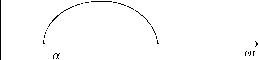 a cot FIGURE 18.3 Different types of trigger signals for switching a thyristor. the supply voltage. The ideal switching signal for a thyristor should have an adequate amplitude of current for sufficient duration with a short rise time as shown in Fig. 18.4. The initial high magnitude and rapid rise of the gate current quickly turn on the device completely. Thus, carriers spread rapidly throughout the surface of blocking junction (/2). This decreases switching losses and increases the initial di/dt capability of the device. After a few microseconds, a small gate current (slightly higher than the minimum value required for triggering Iqj) can be maintained. Ordinarily, a continuous gate signal is not required, but inductive circuits necessitate a sustained gate signal initially, until successful triggering takes place. For reliable operation of controllers, gate trigger signals are normally supphed during the entire on period (e.g., converters of dc drive). Fiowever, for a resistive load, a single sharp rising pulse is sufficient for triggering. For high-power applications, it is a common practice to isolate the control and triggering circuits from the power circuit (consisting of -> I 18.3 Trigger Circuits for Thyristors Normally, thyristors are switched on by the apphcation of a voltage signal at the gate terminal of the device as shown in Fig. 18.1. The gate voltage (vq) is generated with the help of a gate drive circuit, which is called a firing or triggering circuit. Thus, thyristors can be switched on by a slow-rising rectified ac signal, a sharp single pulse, a constant-magnitude dc signal, or a train of high-frequency pulses as shown in Fig. 18.3. The thyristor switches on as soon as Vq exceeds the critical gate trigger voltage (Vqj) level. This depends on the gate-to-cathode junction temperature (Tj), anode current (i), and FIGURE 18.4 An ideal gate current required for a thyristor. - ILLS 5 lus thyristors). Otherwise, the effects of high voltage and high current transients may cause misoperation or damage to the low-power control and trigger circuits. For this purpose, pulse transformers or optocouplers are used for low- and medium-power semiconductor devices. For higher power applications, for example, HVDC transmission systems, fiber-optic cables are used to isolate the control circuit from the power circuit. A 5-mW light trigger power source was found sufficient for switching a light-activated silicon-controUed rectifier (LASCR) with a rating of 4 kV, 3 kA. In general, a thyristor conducts when it is properly biased and the trigger source of a trigger circuit supplies the required the minimum gate voltage (Vgt) Bte current (Iqt)- 18.4.1 Resistance Trigger Circuits A step dc voltage, a slow rising dc signal, or a rectified positive half-wave signal can be used to trigger thyristors. When the voltage applied to the gate terminal exceeds the Vt level, triggering takes place. Figure 18.5 shows a trigger circuit and waveforms for an ac circuit. Before conduction of the SCR, the input supply voltage (v) appears across the SCR. Neglecting R2 and the voltage drop across D, the gate voltage is given by Vr=- Rl + RqK + mii (18.4) 18.4 Simple Gate Trigger Circuits for Thyristors Simple trigger circuits can be realized by R or RC network. They are cheap and consume little power. However, the control and hence the load output voltage (v), are susceptible to the device temperature variations. Moreover, feedback control cannot easily be incorporated. where v = sin cot denotes the supply voltage, and Rq is forward gate-to-cathode resistance. As soon as Vq reaches the Vt ll supplies the required gate current, conduction of SCR takes place. The voltage Vjj coUapses and therefore Vq also reduces to almost zero level, and v appears across the load. Now, R can be increased to reduce Vj and thus to increase a. However, with a larger Rl, eventually the circuit fails to trigger the device as shown by curve 3. Here, the control of a is restricted to 90° only (curve 2 of Vq in Fig. 18.5). Similarly, Iq should not 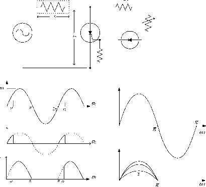 FIGURE 18.5 Resistance trigger circuit for an SCR. exceed the Iqj level. Therefore, the minimum value of the resistor R is given by Rryl <Igm (18.5) This circuit is further improved by adding a resistor R2 across G and К terminals of the SCR. Then the worst-case voltage across R2 should not exceed the Vq level. Therefore, the maximum value of the resistor R2 is given by Rmin + 2 Vrn < Усы (18.6) The same circuit also is applicable for Triac. However, diode Dl has to be removed such that a trigger signal will be available at the gate terminal during both half-cycles. Because the gate of a Triac is not equally sensitive in all four of its modes of switching, a and hence are usually different in the positive and negative half-cycles of the supply voltage. 18.4.2 RC Trigger Circuits A phase-shifted signal in an ac circuit and a slow rising signal in a dc circuit generated by an RC network are used to trigger the thyristors. In these cases the range of a is extendable beyond 90°. 18.4.2.1 AC-Type Figure 18.6 shows a trigger circuit and related vector diagram. The supply voltage appears across the RC branch. Neglecting the discharge of the capacitor during the conduction period of the thyristor, the circuit can be analyzed by the sinusoidal steady-state response of a linear RC circuit. Thus, the phase angle of the capacitor voltage (0), can be controlled from 0° to -МЛг с  -\N\r   FIGURE 18.6 A typical RC trigger circuit. almost 90° (Fig. 18.6). Fiowever, the rms value of the capacitor voltage {Vq), which is equal to {VcosO), decreases drastically for a higher value of в. By variation of R, the phase angle {в) as well as the magnitude of Vq change. The power-factor angle ((/)) of the RC circuit is given by Ф = t-\XJR) = t-\l/(DCR) (18.7) Also, from trigonometry, when в = (n/2) - ф, Ыпв = (1/гшф) and в = tan-\(DCR) (18.8) The instantaneous value of the voltage across capacitor (vq) is given by Vq = 4iVq sin(a;t - 0) = (a/2 У cos d) sin(a;t - d) (18.9) During the positive half-cycle when Vq hence Vq exceeds the Vq level, conduction of the thyristor takes place (Fig 18.6). In fact Vq is the rectified capacitor voltage. Thus, a can be controlled over wide range beyond 90°. By variation of R, phase angle [Q) as well as the magnitude of Vq change as shown in Fig. 18.6. Furthermore, the magnitude of Vq can also be controlled by gate current hmiting resistance R2, as in the case of a resistance-trigger circuit. An improvement in the circuit configuration is possible when the RC branch is connected across the SCR. When the SCR conducts, voltage across the RC branch also reduces to a very low level (ideally zero). The power dissipation in the gate circuit therefore reduces significantly. example 18.2. A 240-V, 50-Fiz supply is connected to an RC trigger circuit (Fig. 18.6). If is variable from 1 to 22 kQ, Vq = 2 V and С = 0.47 iF, what are the minimum and maximum triggering or switching angle (a)? Solution. The phase angle of Vq is given by в = tan (coCi) = tan-\2nfC) = tan (2 x 50 x 0.47 x 10 x R) Furthermore, Vq = У cos 0 and vcot) = V2Vq sin(cot - в). (i) When R = IkQ, it gives в = 8.4°, cosO = 0.989 and Vq = 240 x 0.989 = 237.4 V. Therefore, v,((Dt) = V2VQsm((Dt - 8.4°) = 335.77 sin(a;t - 8.4°) Conduction of SCR takes place at = Vqj = 2 V and (Dt = d. Therefore, vX) = 2 = 335.77 sin(a;t - 8.4°) The minimum value of a is given by ai, = 8.4° + sin-42/335.77) = 8.7° (ii) When i = 22kQ, it gives 0 = 72.9°, cos в = 0.296 and Vq = 240 x 0.296 = 70.97 V. Because vot) = 2 = V2 x 70.97 sin(a;t - 72.8°) = 100.36sin(a;t-72.8°) the maximum value of a is given by a = 72.8° + sin 42/100.36) = 73.9° of the SCR takes place. Simply by controUing R, the charging rate of the capacitor a varies; prevents a large negative supply voltage from appearing at the gate terminal of the thyristor. For a wide range of a, charging of the capacitor is required for almost a three-fourths time-period (T) of the supply voltage. However, for 50 or 60 Hz mains supply apphcations, the foUowing empirical equation had been reported: RC>0.65T = 4/a; (18.10) where the angular frequency of ac mains со = In/T. The value of R2 Vqj are supplied to the gate terminal: is chosen such that the required Iqj and 18.4.2.2 Half-Wave Type This circuit has been realized by incorporating an additional diode (d2) in the circuit shown in Fig. 18.6. As iUustrated in Fig. 18.7, the capacitor is charged (upper plate negative) by v through D2. The charging starts from the negative-zero-crossover instant to the negative peak of v, that is, - a/2 V. Then the voltage at the anode of D2 (i.e. v) becomes equal to the voltage at the cathode (i.e. v), therefore the current through D2 ceases and D2 becomes reverse-biased. Now the charging of the capacitor (with upper plate positive) takes place through R and the charging rate depends on the time-period RC. When Vq (rectified Vq) becomes shghtly higher than Vqj, conduction iA/W 0 (:йллл ©  FIGURE 18.7 Another RC trigger circuit. R2< V-Vqt Vj) (18.11) where v is the voltage at the switching instant of thyristor and is forward voltage drop of diode . Also, the maximum value of R2 is given by 2max - V2V-Vgt-di V2V (18.12) With an approximation, the previous analysis of the trigger circuit holds good even for this case. 18.4.2.3 Full-Wave Type This circuit has been realized by incorporating a diode bridge in the previous circuit (Fig. 18.6). As illustrated in Fig. 18.8, charging of capacitor takes place through R and the charging rate depends on RC (time period). When Vq (rectified Vq) becomes shghtly higher than Vqj, conduction of SCR takes place. Simply by controUing R, the charging rate of the capacitor a varies. In this circuit, charging of the capacitor starts from each zero-crossover instant and the capacitor experiences only a half-wave rectified voltage until the thyristor is triggered. The circuit can be analyzed by the complete response of an RC circuit with a sinusoidal (half-wave) excitation. The voltage expression is given by v{t) = sin cot = Ri{t) + (1/C) Kt)dt where differentiating. o< t>- = - 2 CO (DVCOS(Dt = R-- (18.13) С (18.14) 1 ... 38 39 40 41 42 43 44 ... 91 |
|
© 2026 AutoElektrix.ru
Частичное копирование материалов разрешено при условии активной ссылки |