 |
 |
 |
| Главная Журналы Популярное Audi - почему их так назвали? Как появилась марка Bmw? Откуда появился Lexus? Достижения и устремления Mercedes-Benz Первые модели Chevrolet Электромобиль Nissan Leaf |
Главная » Журналы » Metal oxide semiconductor 1 ... 39 40 41 42 43 44 45 ... 91  Load Solution. Because (i) When = 1 kQ, it gives ф = 81.6°.  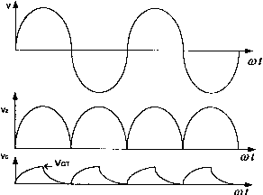
FIGURE 18.8 Full-wave RC trigger circuit. With zero initial condition, the total current response is given by i{t) = (V/Z)[sm(a)t + (/))- sin (/) exp(-a)t/ tan ф)] (18.15) VR(t) = Kt)R = (VR/Z)[sm(cot + ф) -зтф- exlp(-CDt/tanф)] (18.16) = cos ф[sm(at + ф) - 8тф exp(-cot/ tan ф)] (18.17) Also, VQ(t) = V(t) - Vjt), or Vc{(Ot) = v(C0t) - VjCDt) (18.18) As soon as i; reaches the Vqj level, triggering of the thyristor takes place. Example 18.3. If the RC branch of Example 18.2 (Fig. 18.6) is used in a full-wave trigger circuit, what are the minimum and maximum firing or switching angle, a? Vc{t) = v(t) - Vjit) = sin cot - cos Ф X [sin(a;t + ф) - sin ф exp(-cot/ tan ф)] therefore, i;(cot) = V[sin cot - cos (/){sin(cot + Ф) - sin (/) exp(-cot/ tan ф)}] = a/2 x 240 X [sincot - cos(81.6°){sin(cot + 81.6°) - sin(81.6°) exp(-cot/ tan(81.6°))}]. Now the value of Vc(a)t) can be computed for cot = 0 to 180° by the direct substitution method. The required value of cot = a corresponds to the condition when Vq becomes equal to Vqj = 2 V. It gives cot = ain = 2.5°. (ii) When = 22 kQ, it gives ф = 17.Г. Therefore, i;(cot) = a/2 X 240[sin cot - cos(17.r){sin(cot + 17.1°) -sin(17.1°)exp(-cot/tan(17.1°))}] It gives cot = anax = 11-35°. 18.4.3 Diac Trigger Circuit This circuit is commonly used for Triac where the trigger signal is required in both half-cycles of the supply voltage (Fig. 18.9). Basically, it is similar to an RC trigger circuit (Fig. 18.6). FLere both SCR and diode D are replaced by a Triac and a Diac, respectively. The capacitor is charged through the resistance R during each half-cycle. When reaches the breakover voltage of Diac {Vq = 30 V), conduction of Diac takes place and the required gate current is supplied. Triac conducts and voltage across the capacitor (hence Vq) collapses for the remaining portion of the half-cycle. In the next half-cycle the same phenomenon repeats. FLere, Triac conducts in positive half-cycle by positive gate current and in the negative half-cycle by the negative gate current. Thus, Triac operates in the first and third modes of its switching characteristics. Fiowever, the gate sensitivity of Triac is not the same in both these modes. Therefore, for commercial circuits, an additional RC branch is added between the capacitor and Diac to make a the same in both half-cycles. In this circuit the charging of the capacitor starts from each zero-crossover instant of the supply voltage, and the RC circuit experiences only a half-wave voltage before triggering of the thyristor. The circuit can be analyzed by the complete response of an RC circuit with a sinusoidal (half-wave) excitation as discussed in the previous section.   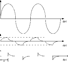
FIGURE 18.9 A Diac RC trigger circuit used in ac regulators. example 18.4. If the RC branch of Example 18.3 (Fig. 18.6) is used in a Diac trigger circuit (with Yq = 30 V), what are the minimum and maximum firings or switching angle a? Solution. Equation (18.18) for Vq holds good even for this case. However, here, triggering takes place at Vc((ot) = Vcioc) = Vjq = 30 V instead of Vt = 2 V. Now, the value of Vc((Dt) can be computed for cot = 0 to 180° by the direct substitution method as was done for the previous case. A simple computer program in QBASIC is given in what foUows for Diac trigger circuits to find the required value of a. It corresponds to the condition when Vq becomes equal to Vq. REM Program for switching angle. Alpha in Diac trigger circuit PRINT Program developed by Jamil Asghar, EED,AMU,Aligarh, India PRINT Give: R in K-Ohm, С in uF, VBO of Diac, Supply Voltage INPUT R, C, VBO, V pi = 4 * ATN(l) phi = ATNdOOO / (2 pi * 50 R C) ) Vm = SQR(2) * V phid = phi * 180 / pi FOR wtd = 0 TO 180 STEP 0.1 phi = pi * phid / 180 wt = pi * wtd / 180 vRl = SIN(wt + phi) - SIN(phi) * EXP(-wt TAN(phi)) vR = Vm * vRl * COS(phi) vC = Vm * SIN(wt) - vR IF vC >= VBO GOTO 33 NEXT wtd IF wtd >= 180 THEN PRINT NO TRIGGERING - VALUE OF RC TOO HIGH GOTO 4 4 33 PRINT For diac: R in kOhms = , R, C -in uF= , C, VBO = , VBO PRINT Alpha in deg.= , wtd, Phi -in deg= , phid, vC= , vC 44 STOP END Result: (i) R=lkQ, Value of alpha =11.33° (ii) R=22kQ, Value of alpha =46.5° 18.4.4 AC-Thyratron Type Trigger Circuit This trigger circuit is simUar to the circuit shown in Fig. 18.6, except that the phase-shifting RC network is energized from a separate center-tapped transformer. A simple RC trigger circuit is disadvantageous in that does not remain constant for aU values of в (Fig. 18.6). Therefore, for higher values of 9 (near 90°), becomes very smaU eventually faUing to trigger the thyristor. Thus the control range of a becomes smaU. While in this case the rms value of the voltage remains constant and its phase angle P varies from 0 to almost 180° (lagging) as shown in Fig. 18.10. From the phasor diagram of the secondary of the transformer and the RC circuit. Z ADB = п/2-ф = в and Vqa = У( therefore. ф = I BAG = я/2 - Z ADB = Z ABO Also, from triangle OAB, (18.19) (18.20) = 71 - 20 = 2(я/2 -ф) = 2в = 2tan (coCR) 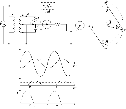 FIGURE 18.10 An ac-thyratron type trigger circuit. The same circuit can also be used to trigger two thyristors in a bridge. In this case, gate current flows during the entire conduction period of the thyristor. It unnecessarily increases the temperature of gate-to-cathode junction (T, which may reduce the voltage withstand (blocking) capability of the thyristor. 18.4.5 Unijunction Transistor-based Trigger Circuit A unijunction transistor (UJT)-based oscillator provides constant-frequency, sharp pulses with small rise-time. The UJT is a three-terminal, two-layer PiV device (Fig. 18.11). It has an iV-type semiconductor (between two base terminals and B2) with a small P-type doping (at emitter terminal E). The emitter terminal divides the interbase resistance (V) into two parts (say, R and Rb2)- If biasing voltage (V) is applied across the base terminals, the voltage in iV-type material near emitter terminal (k) is given by Vfi = Rв^ R (18.22) When the emitter voltage {v) is less than (or цУ), the emitter-Bl junction behaves as a diode in the reverse-biased condition, and thus it offers a very high impedance. A small reverse leakage current (few microamps) flows through the emitter terminal. A UJT oscillator is shown in Fig. 18.11c. When a dc supply voltage (Vg) is connected, charging of the capacitor starts through resistance R and R. The voltage across the capacitor Vq {or v) increases. As soon as shghtly exceeds the or {цУв + d) level, the P-iVjunction behaves as a diode in the forward-biased condition. Then emitter to basel impedance collapses and the flow of through R takes place. The capacitor is discharged through R and therefore a voltage pulse appears across R (Fig. 18.1 Id). At the trailing edge of the pulse, becomes very small (valley voltage V), depletion layer forms again and the P-iV junction (between E and Bl) becomes reverse-biased. Ideally, no current flows between E and Bl terminals (except the reverse leakage current) and they behave as open-circuited. Now charging of the capacitor starts and again increases. The charging rate depends on (Pin + P)C and the discharge rate of the capacitor depends on RC. The delay period (т^) and the time period (t) of the pulse are given by where t] is called the intrinsic-standoff ratio of UJT and its value is less than unity (typical value varies between 0.5 and 0.85). T = Ti+PiC (18.23)
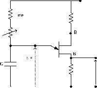 (а) UJ structure (b) qui alent circuit model (c) UJ oscillator  cot (d) Wa e forms of oscillator 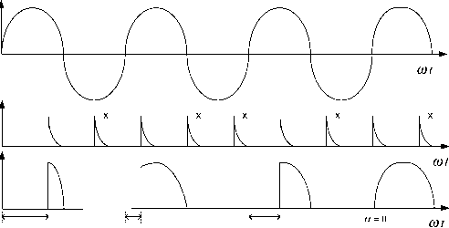 a a a (e) Unsynclironised tri er pulses with dc biasin olta e. FIGURE 18.11 A UJT-based oscillator circuit and waveforms. (18.24) Also, the switching angle depends on the delay period of the osciUator, which is given by a = ШТ (18.25) However, in a trigger circuit, a may not be equal in each cycle of the supply voltage {v) as shown in Fig. 18.1 le. Some pulses arrive when the thyristor is already conducting whUe some arrive when the thyristor is in the reverse-biased condition; these pulses are marked x. They make no contribution toward triggering of the thyristor. Thus, a does not remain the same but varies randomly in each cycle. To get a constant value of a, synchronization of the trigger pulse with supply voltage is necessary. Figure 18.12 shows a UJT-based trigger circuit 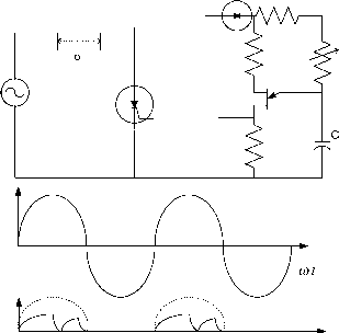 к к ГУ >   (b) cot FIGURE 18.12 a ujt trigger circuit with waveforms. synchronized with mains voltage (v) through a diode bridge. The charging of the capacitor starts from each zero crossover instant only. The first pulse in each half-cycle that triggers the thyristor is synchronized with v, and therefore a becomes equal in each cycle. By controlling R, the time period of oscillator (t), or the delay period of the first pulse (т), a can be adjusted. The UJT trigger circuit may also be energized from a separate transformer (for biasing) and the same performance can be achieved. 18.4.5.1 Design Considerations Selection of P. It should be low enough to prevent undesirable triggering of the thyristor. Therefore, Ri is related to the maximum gate voltage ( Vgd) that will not trigger the thyristor at any temperature: Vgd> Pi + 2 + R (18.26) -BB(min) Selection of 2- It is selected from the stability consideration of the circuit because Vp decreases with temperature. The follow- ing equation gives the approximate value of R2 for compensation over a temperature range of 40 to 100°C: R, = (18.27) Selection of capacitor C. It should store sufficient charge to trigger the thyristor. The typical values are between 0.01 to 0.7 iF. It can be calculated with the help of Eq. (18.22). The time period т of the output pulse is + PC, while the delay period that corresponds to the switching angle (a) is т^, as given in Eq. (18.24). Selection of Р^ш- It should be large enough so that the load line formed by P and Vb intersect the emitter characteristics of UJT to the left of the valley point. Therefore, min > Vrr - Vv (18.28) Selection of P. The total charging resistance (P + RJ must be sufficiently small to allow peak point current drawn from the supply. Therefore, max - + min Vbb - Vp (18.29) Example 18.5. Parameters and ratings of a UJT (2N2646) at Tj = 25 °C are given below: Maximum interbase voltage (Vg) = 35 V Maximum average power dissipation = 300 mW Range of interbase resistance (P) = 4.7 to 9.1 kD (typical 5.6 kD at Vbb = 12 V) Valley point current /у = 4 mA at Vbb = 20 V Intrinsic standoff ratio, rj = 0.56 to 0.75 (0.63 typical) Valley point voltage Уу = 2 V at Vbb = 20 V Peak point current /p = 5 iA (maximum) at Vbb = 25 V The maximum gate voltage {Vqj) that will not trigger on the SCR= 0.18 V Design a suitable UJT-base trigger circuit for a single-phase-controlled converter (rectifier) operating with 50-FLz ac mains supply. solution. The switching angle a varies from 0 to 180°, that is, for half time-period of the ac mains supply. Therefore, T 2 2 X 50 = 10 ms Let = 12 V. Then Vbb - Vy 12-2 4 X 10-3 = 2.5 kQ Take ii, = 2.7 kQ (ii) Vp f]VBj = 0.63 X 12 V = 7.56 V, Ip 5 X 10⁻⁶ Then the value of R is given by R = Rm- min = 888 - 2.7 = 885.3 kQ Take R = I MQ; then the new value of R = 1002.7 kQ. (iii) Selection of Base-Resistances. The empirical formula for R2 is given by 10,000 10,000 Therefore, the nearest value is taken R2 = 1.2 kQ. Then Rl can be found as il + + R BB(mm) Rl < 0.18 Rl + 1200 + 5600 It gives Rl less than 103 Q; therefore take i = 100 Q. (iv) Selection of Capacitor. Let the triggering circuit be designed for a maximum delay period (1 ) of 10 ms. The maximum delay period corresponds to the minimum frequency of the osciUator, which is given by Therefore, T = 10 ms = RCln 10-2 10-2 = 0.01 iF 1002.7 X 10 X Although a capacitor of 0.01 iF can be selected, the pulsewidth of the triggering pulse wiU be smaU {R2C = 100 X 0.01 = 1 iF). However, this may not be sufficient to trigger a thyristor successfully. Then it should be increased (about 5is). Moreover, sometimes the voltage pulse across Ri is not sufficient to drive the thyristor; then the value of Ri may be increased. The minimum delay period is given by min = min X С X In X 0.99425 = 0.0268 ms The minimum value of a = minimum delay period (in ms) x = 2.7 X 10 X 0.01 X 10- 360° 20 ms 0.0268 X 360 = 0.483° SimUarly, the maximum delay period is given by 1 max - max X С X 1п I -Г] = 1002.7 X 10 X 0.01 X 10- X 0.994 = 9.967 ms The actual maximum value of a = maximum delay period (in ms) x 360° 20 ms 9.967 X 360° 20 = 179.4° 18.4.6 Advanced Triggering Circuits for Thyristors Although RC trigger circuits are very simple and economical, they depend on gate trigger characteristics of the thyristor used, and they cannot be used easily in self-programmed, automatic or feedback controUed systems. Because the use of power-electronic controUers is increasing steadily in industry as weU as in power systems, different types of controUers are required for specific apphcations. In a controUer, a group of thyristors or power-semiconductor devices are required to be switched at different switching instants for different durations and in a particular sequence. Different three-phase converters, for example, dual converters, cycloconverters, and regenerative reversible drive, may require 12 to 36 such devices. Thus, switching a large number of these power devices with different control strategies by a simple trigger circuit becomes almost impossible. Moreover, incorporation of feedback and/or different control approaches for same load/drive system requires an inteUigent controUer. Therefore, the advanced triggering circuits become necessary. Some modules of power semiconductor devices include a gate drive as weU as transient protection circuitry. Such commercially avaUable modules are caUed intelligent module or smart power. They include input-output isolation and gate drive circuits, microcomputer control, a protection and diagnostic circuit (for overcurrent, short-circuit, open load, overloading and excess voltage) and a controUed power supply. Similarly, custom-built driver integrated circuits (ICs) are also available for thyristors as well as MOSFETs and IGBTs. 18.4.7 Buffer and Driver Circuits for Thyristors In most power electronic circuits, a difference of potential exists between the gates of the various thyristors as well as between the control circuit and thyristors. The control electronics normally consist of linear ICs (e.g., operational amplifiers, timers) and digital ICs (e.g., TTL, CMOS), discrete passive elements, and active devices. Basically, they are low-voltage (few tens of volts) and low-power (few watts) circuits. The power circuit that consists of thyristors is a high-voltage circuit (normally of the order of several hundreds of volts). Therefore, it becomes necessary for the output channels of the gate-pulse generating circuit to be isolated from one another as well as from thyristors. The isolation can be provided either by a small high-frequency pulse transformer or by an opto-coupler 1С. Then it becomes possible to switch on several thyristors simultaneously (e.g., in a series connection or switching an ac load by two antiparallel thyristors). Similarly, control electronics, which control the conduction period of each thyristor, give an output of very low power (few milliwatts, for example the output of a CMOS logic gate). In general, in most cases output power is not sufficient to drive the gate directly. Therefore, an amplifier circuit is required that amplifies the weak gate drive control signal. For this purpose, a transistor amplifier is used. For isolation between control and power circuit, the use of a pulse transformer is common. Normally, it has two or three windings, and it is a small low-power and high-frequency transformer; the turns ratio are normally 1:1 or 2:1. When a high-frequency pulse is applied to the primary winding, an output pulse appears at one or more output secondary windings. The optocoupler 1С circuit is also used for this purpose. In this arrangement, an infrared hght-emitting diode (I-LED) turns on a photosensitive device (photo-SCR, photo-Triac, photologic gate, or phototransistor), which ultimately turns on the thyristor. Fiowever, a separate dc power supply is normally required for each thyristor. For high-voltage applications, the optical-fiber technique is applicable. In this case, the output of the control electronic circuit is supplied in the form of a light signal through the optical-fiber cable to the thyristor. Optical fiber offers a very high level of insulation between the control circuit and the power circuit consisting of thyristors. Figure 18.13 shows different driver and buffer circuits (DBC). In Fig. 18.13a, pulses are generated by a differentiator circuit (PiQ), which converts a step input signal into sharp positive and negative pulses. The positive pulse is then amplified by a transistor amplifier circuit. The isolation is provided by a pulse transformer. Diode D3 allows only the positive portion of the amplified signal to be applied between gate and cathode terminals of a thyristor; D2 provides a freewheeling path for the inductive current of the primary winding of the pulse transformer. This protects the transistor from the high-voltage spike (Ldi/dt) that could be generated due to the snap of inductive current by the turn-off of the transistor. The anode current of a thyristor reaches the latching current level after a certain delay period. Therefore, for an inductive load, a long pulse is required for successful triggering. For this purpose, the triggering pulse is stretched by connecting a capacitor in parallel with However, to avoid saturation of the core of the pulse transformer due to stretched unidirectional current, the pulse duration is restricted to 50 to 100 is. Often in converter circuits with inductive loads the load current is discontinuous within the assigned conduction period and therefore it is required to trigger the thyristor more than once. Similarly,the conduction period (or commutation instant) of each thyristor depends on the load current flowing through it, which varies with respect to the load power factor. Therefore, for reliable triggering, a continuous gate signal is required but it increases thyristor losses and decreases voltage withstand or blocking capability. Alternatively, a train of trigger pulses of high frequency (e.g., 10 kFiz) is supplied during the entire conduction period. In this case the switching may be delayed by one time period (0.1ms for a 10-kFiz signal) of the pulse train. Fiowever, this delay is negligible for power frequency (e.g., 1.8° for 50Hz or 2.0° for 60 Hz). Figure 18.13b shows a commonly used driver and buffer circuit (DBC). A high-frequency (5 to 20 kFiz) positive pulse (or square-wave signal) from an oscillator is applied to an AND gate continuously. These pulses are allowed to reach the base of transistor only when the input drive control signal is high. The transistor basically acts as a switch to energize the primary winding of the pulse transformer corresponding to each pulse. Moreover, these pulses also are amplified. Their magnitudes are restricted by the current-limiting resistor (R2) connected in series with the dc source. In the secondary windings pulses of almost the same strength are produced due to transformer action. Due to the snap of inductive current in the primary winding (when the transistor is switched off), a negative pulse is also generated in the secondary winding. This pulse is blocked by the diode D2. Thus amplified positive pulses become available between G and К terminals of the thyristor. Figure 18.13c shows an optocoupler 1С chip-based isolation circuit. An infrared light-emitting diode (I-LED) and a photo-SCR are fabricated in a single 1С chip. On arrival of the input drive control signal, I-LED conducts and emits light to bring the photo-SCR into the conduction mode. Thus switching of the main SCR takes place. Figure 18.13d shows another optocoupler-based circuit where a phototransistor is used. Because the output of the phototransistor cannot drive a thyristor, an additional transistor (BJT) is used for amphfication. This type of circuit requires an additional electrically isolated dc power supply for each thyristor.   -►h I I Input ate control si nal 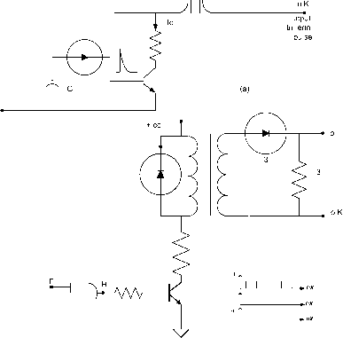
FIGURE 18.13 (a) Driver and buffer circuits for thyristors; (b) driver and buffer circuit in common use. Figure 18.13e shows a fiber-optic cable-based driver circuit. It provides the very high electrical isolation and large creepage distance required between a low-power control circuit and a high-voltage power circuit. In the case of an optocoupler, I-LED and the receiving phototransistor both are fabricated on the same 1С chip. Therefore, capacitance between them should be as smaU as possible to avoid retriggering at both turn-on and turn-off of the power devices (e.g., power transistors, power MOSFET and IGBT), because of the jump of potential across the devices (dv/dt). To avoid this problem, the fiberoptic technique is used. The first amphfier is a receiver (fiber optic integrated detector/preamphfier), and the second amplifies the control signal to the required level for triggering of the thyristor. Here, the driver circuit is linked to the control circuit only through the fiber-optic cable, thus galvanic isolation is provided between them. Example 18.6. Design a suitable pulse transformer-based driver circuit for gating a given SCR. The worst-case requirements of the SCR are given in the following: /cnin = 100 mA, Va = 2.5 V@ - 65 °C The input drive control signal is an output of AND gate (IC7408). The specification of a TTL gate (general type) is given by Output current and voltage at the logic 1 level: I = 0.4 mA, @Vqh = 2.4V, and Output current and voltage at the logic 0 level: I = 16 mA, @VoL = 0.4V Solution. The gate current requirements of the thyristor are important for design considerations. Then the Input dri e control si nal  pto-coupler with photo SC Input dri e control si nal + cc pto-co iJ pie r with photo transistor  J Input dri e control si nal 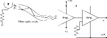 FIGURE 18.13 (c) optocoupler 1С chip-based isolation circuit; (d) optocoupler with phototransistor; and (e) optical fiber cable-based driver circuit. desired gate current and hence the secondary current of the pulse transformer (/2) should be 100 mA. Let the turns ratio of the pulse transformer be 2 :1 (Fig. 18.13b). Therefore, the primary current (J) of the pulse transformer can be taken as /i = - = 50 mA FLere, the maximum output current of TTL 1С is limited to 0.4 mA for logic 1 level. Neglecting the small Ve voltage drop during the switching of the transistor. Rb> 0.4 X 10 = 6kQ We thus choose = 6.8 kQ. For this purpose, a switching transistor (ВС 107, ВС 148, BELIOON, 2N222 or similar) may be selected according to voltage and current ratings (У^с c)-Let BELIOON (or SL 100) transistor be taken whose specifications are Vcbo = 60 V(,), Iq = 500 mA(,), hy (at /с = 150 mA, Vqe = 1V, = 25 °C) = 50 to 280. Because the required primary winding current of the pulse transformer 1=1 = 50 mA, the value of resistor Rl (which is used to limit the collector current within the allowable range) is given by Vnn 12 Ri = cc Ic 50 X 10 = 240 Q Then we choose R = 220 Q. resistor = IqRi = The power rating of (50 X 10- f X 220 = 0.65 W. Therefore, a 220-Q, 1-W resistor will be a good choice. 18.5 Drivers for Gate Commutarion Switches Devices from the thyristor family differ from those of the transistor family with respect to their input or drive characteristics. In the case of a thyristor, once it is triggered it continues to be in the same mode unless current through it reduces below its holding current level. However, in the case of transistors, to keep them in the conduction mode, a continuous base or gate signal is required. Basically, transistors or other gate commutation devices are either current controlled (e.g., BJT) or voltage controlled (e.g., MOSFET, IGBT). Similarly, for turn-on operation, GTO behaves as an SCR, while the turn-off operation (or gate current requirements for turn-off) is totally different from the SCR. A GTO requires a large negative gate current and a high power sink for successful commutation (similar to driving requirements of power BJTs). As discussed earlier, normally the driver circuit has to provide an electrically isolated gate/base signal. For the power BJT, the current gain (h or P) of the transistor is low ( = 5 to 10). Therefore, the power capability of the driver circuit should be as high as 20% of the power circuit. However, driving a power MOSFET is similar to driving a very high-impedance capacitive network, thus a carefully designed very low power drive circuit is required. Most gate-voltage-controlled (or gate-commutation-controlled) power semiconductor devices require a very low power driver circuit. Normally, a unipolar drive signal (a positive voltage pulse) is sufficient for normal turn-on and turn-off of the devices. However, for rapid turn-on and turn-off, bipolar signals (both positive and negative voltage pulses) are required. Moreover, for high switching performance, similar circuits with high (source and sink) capabilities are required for MOSFET, IGBT, and BJT alike. For MOSFET/IGBT, the transition current capability should be high (with low output power). However, for BJT, a sustained high base current (in the high output power) is required. For GTO, a very low power circuit is required for turn-on. However, the turn-off circuit capability should be very high (compatible with the power BJT drive circuit). Although it is required for a very smaU period, the gate power requirement of the negative pulse is about one-third of the power circuit. 18.5.1 Gate Drive Circuits for Power MOSFETs The input gate characteristics of a MOSFET differ from its bipolar counterparts. The gate is isolated electrically from the source by a layer of sihcon dioxide. Ideally, no current flows into the gate when a dc voltage is applied. However, a smaU leakage current (of the order of 10 A) flows to maintain the gate voltage and also during the transition periods (off-to-on and on-to-off). Therefore, a smaU current is enough to charge and discharge the device capacitances. However, the device 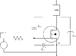 (N-channel nhancement type M SF FIGURE 18.14 An N-channel enhancement-type MOSFET with voltage-dependent device capacitances. capacitances and gate-drive source impedance determine the device switching speed. There are three capacitances and they are nonlinear and voltage-dependent (Fig. 18.14). If the gate voltage is reduced to zero for turn-off operation, Vp)s attains the supply voltage magnitude (V), the potential at D swings from 0 to Vp)p) and Cj is charged up to to Vp (say, 100 V) through a low gate source impedance (R) as shown in Fig. 18.15a. Now if a gate drive signal is applied (higher than the threshold value), the device will be on. Ideally, the voltage across D and S reduces to zero (neglecting smaU V) and terminal D will swing to ground potential (which earlier was at Vjj = 100 V). The decreasing V produces a feedback current (i = Cg dVjg/dt) through Cj to the gate circuit as shown in Fig. 18.15b. This feedback mechanism is called the MiUer effect. Thus, the source and sink capabUities of the gate drive are required: (i) due to the charging and discharging of C; and (ii) due to the large swing in the gate-to-drain voltage. Although C is an important parameter, Cj is more significant due to the MiUer effect. As the source resistance (R) is in series with C and Cj, the turn-on time and the turn-off time are affected by this resistance. Therefore, both periods can be controUed independently (Fig. 18.16). SimUarly, a bipolar gate drive signal allows rapid turn-on and turn-off. Low-power digital logic circuits (TTL or CMOS) can easily be used to drive directly the gate of power MOSFET (Fig. 18.17). Because CMOS has limited source current and sink current capabilities (2 and 4 mA @ Vp = 12 V respectively), the modest delay in rise time and faU time are expected due to the MiUer effect (charging and discharging current requirements). However, the CMOS 1С can directly drive the gate with required magnitude of the drive voltage. For a TTL device with a totem pole output, the output voltage available is approximately 3.5 V (when V = 5V). This voltage (3.5 V) may be insufficient to drive the MOSFET into the conduction mode. However, TTL has better source and sink capabUities than its counterpart CMOS, which speeds up the switching 1 ... 39 40 41 42 43 44 45 ... 91 |
||||||||||||||||||||||||||||||||||
|
© 2026 AutoElektrix.ru
Частичное копирование материалов разрешено при условии активной ссылки |