 |
 |
 |
| Главная Журналы Популярное Audi - почему их так назвали? Как появилась марка Bmw? Откуда появился Lexus? Достижения и устремления Mercedes-Benz Первые модели Chevrolet Электромобиль Nissan Leaf |
Главная » Журналы » Metal oxide semiconductor 1 ... 40 41 42 43 44 45 46 ... 91 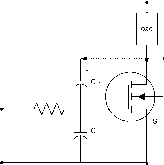 -алл/- 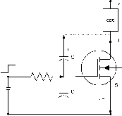
FIGURE 18.15 Large voltage swing at D: (a) during turn-off; and (b) during turn-on. transition and reduces turn-on and turn-off times. Thus the output vohage magnitude can be raised by the open-collector TTL device with a pull-up resistor connected to a separate + 10 to +15V dc power supply. It can guarantee rapid gate turn-off due to large sink capability when the output transistor of TTL (inside the TTL 1С) is conducting at the logic 0 level (Fig. 18.17). Moreover, this arrangement ensures sufficient gate voltage (10 to 15 V) to turn on the MOSFET fully Fiowever, the turn-on is not as rapid as turn-off because the pull-up resistor delays charging of the device capacitor C. Figure 18.17a shows a CMOS-based driver circuit. The output voltage (+10 to +15 V) of CMOS logic is large enough to drive the MOSFET. To increase source and sink capabilities CMOS buffers (CD4049 and CD 1450) are used. Thus performance is achieved with respect to switching speeds and low output impedance. To increase the switching speed further, more buffers can be connected in parallel to increase the sink current capabilities for fast turn-off. Figure 18.17b shows the connection of an open-collector TTL-based driver circuit. The drawback of the TTL output due to its lower magnitude of output (which is the input drive control signal) has been removed. Although an additional dc power supply (+10 to +15 V) will be required, this provides rapid turn-off and ensures sufficient gate voltage to turn on the MOSFET fully. Input dri e control circuit  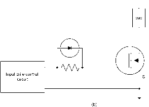 FIGURE 18.16 Driver circuits for (a) delayed turn-on; and (b) delayed turn-off Figure 18.17c shows a configuration for fast turn-on with reduced power dissipation in TTL. When the TTL output is at the logic 1 level, transistor Q2 conducts. The output point (cathode of diode and base of Q2) comes to about the ground potential, and Q3 remains in the off state. A very small power loss (few milliwatts) occurs in R whose value is large, and it behaves as base resistance of Q3. Similarly, when the TTL output is at the logic 1 level, Q3 conducts due to the high voltage at its base and the diode becomes reverse-biased. Thus a high voltage (approximately 12 V) reaches the gate of the MOSFET. The conducting Q3 provides a lower source impedance than R (as in the previous case. Fig. 18.17b). Thus the source capability increases, which enables a fast turn-on. The turn-off period depends on the conduction of the TTL output or pull-down transistor Q2 (by shunting the input gate capacitance of MOSFET to ground). Although the sink and source capability of different types of TTL families varies, the 74AC00 series (logic type) offers better performance for driving the MOSFET. The typical source current and sink current are 24 mA with a 7-ns propagation delay. Only the Schottky (74S00 series) and the low-Schottky (74LS00 series)
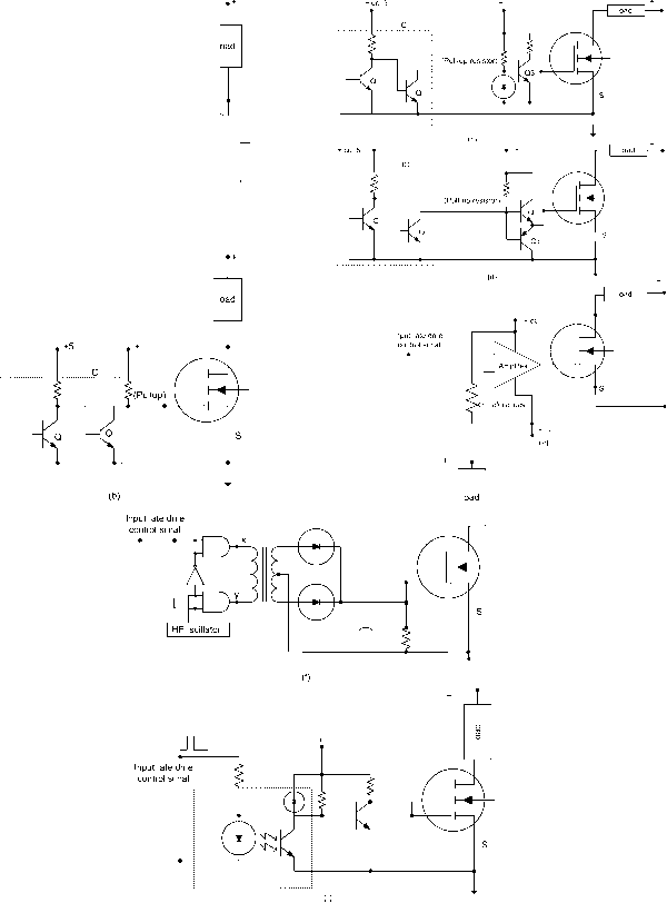 FIGURE 18.17 (a)-(g): CMOS and TTL IC-based driver circuits for MOSFET offer less propagation delay (4 ns) but their source and sink current magnitudes are significantly low. Figure 18.17d shows an open-collector TTL driving a complementary emitter follower (push-pull configuration). This circuit removes the drawback of the lower sink capability of the previous circuit (Fig. 18.17c). Thus, very fast turn-off (hence high switching speed) is attained by using an outboard transistor (Q4) to clamp the gate-to-ground. Both Q3 and Q4 are operating as emitter followers. As they are never driven into saturation, their associated storage times do not significantly affect the switching frequency limit of the gate drive circuit. Figure 18.17e shows a bipolar driver circuit, where during on and off periods, the input drive signal varies between + V to - Vc- This type of driver circuit is required for fast switching applications. In this case the turn-on time and turn-off time are small and the configuration is similar to a complementary emitter-follower circuit. FLere, source and sink capabilities are increased by providing low output impedance of the operational amplifier. Due to the negative voltage rail ( -V), the input gate capacitor of MOSFET discharges quickly and hence the turn-off time decreases. Figure 18.17f shows a pulse transformer-based driver circuit. The pulse transformer provides the isolation needed to drive the MOSFETs at different voltage levels (e.g., in a bridge configuration) or to control an iV-channel MOSFET driving a grounded or source-follower load. The size of the transformer reduces significantly when the operating frequency becomes very high (100kFLz or more). As current and hence the power requirement for the gate driver circuit is very small at steady-state condition (few microwatts only), a separate driver circuit and additional independent dc power supply are not required. Fiowever, at the dynamic condition, that is, during turn-on or turn-off transitions, large current (high source and sink capability) is required for fast switching. Another limiting factor is the switching capability of the diode. Thus the Schottky diode can be used because its turn-off time is very small (about 0.23 is). Fiere, the high-frequency carrier signal reaches the logic gates when the input drive control signal is high. The output voltage of logic gates become alternately high and low, and therefore current flows in the primary winding of the transformer from xto у and vice versa. Thus ac voltage, generated in the secondary winding of the transformer, is rectified and filtered. This dc voltage is ultimately used for driving the gate of a MOSFET. Recently, instead of a pulse transformer, a miniturized coreless (planar) transformer of about 1 cm, fabricated on a printed-circuit board, was used at 1 MFiz for the same application Figure 18.17g shows an optocoupler-based electrical isolation circuit. This circuit is similar to the optocoupler-based driver circuit discussed for the thyristor (Section 18.4.7). Moreover, custom-built integrated driver circuits are also available for such applications. Figure 18.18 shows connections of the DS0026 or MMH0026 clock driver, which has been designed for high capacitive loads (high sink and source Input ate dri e q si nal from 1С 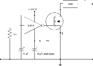 FIGURE 18.18 The DS0026 cloak driver as driver for MOSFET capability). It has a capability of ±1.5 A output peak current (source and sink) with a typical 15-ns propagation delay, and is compatible with series 54/74 TTL devices. Similarly, a large range of such custom-buih integrated driver circuits are also available for such applications. 18.5.2 Design Considerations of MOSFET Driver Circuits Normally, manufacturers do not specif) the device capacitances (Fig. 18.14), rather they quote input, output, and reverse common source capacitances (Q, and Q, respectively). All these capacitances are related according to the following: Qss - ds ~l~ Q<i where shorted where C shorted Qss - Q( (18.30) (18.31) (18.32) The device switching speed depends largely on (or Cj) and the gate drive source impedance. Fiowever, two considerations make accurate estimation of switching time (turn-on and turn-off) difficult. First, the magnitude of Q varies with 2)5, particularly large variation at low drain voltage levels. The switching time constant (RC) determined by Q and gate-drive impedance changes even during the switching cycle. The second consideration is due to the Miller effect. The switching transition can be divided into three distinct periods as shown in Fig. 18.19. The gate drive requirements for these three periods may be expressed as follows: in = Qcc V( iss GS{Th) /ih - to) 05(011) /(t2 - h) for tQ < t <ti for tl < t < t2 = Qss{(GS(on) - VGS(Th))}/(t3 - h) for t2<t<t,  FIGURE 18.19 load. Ideal switching characteristics of MOSFET with resistive A higher-value gate resistor may efficiently damp out the osciUation but simultaneously it slows down the switching speed of the MOSFET. Because most of the driver chips operate from a 12-V source, they supply or absorb about 1A or more during the switching transitions. Therefore, 12 Q is a suitable upper value for the gate resistance to damp out oscillation. However, the gate drive circuit response wiU be faster when it is an underdamped circuit. Therefore, if a smaU overshoot, say, 10%, is aUowed, then the corresponding value of С = 0.6 (which is found from the universal response curve of a second-order underdamped circuit) is obtained. Therefore, The value of capacitances may be found from the manufacturers data book. For the first two periods, Q and values may be assumed corresponding to Vj = fDD-WhUe for the third period, assume Q corresponding to DS = DS(on)- A smaU-valued gate resistor of considerable power rating (5 to 20-W range) is used in high-speed switching circuits. This is because the stray inductance of the device assembly connecting wire from driver circuit/chip (on printed circuit board to the gate of MOSFET) and the gate capacitances cause osciUation of input gate current. It behaves as an underdamped series RLC circuit. If there is no gate resistance on the gate driving circuit (ideally), then undamped oscillation wiU cause a gate voltage (Vq) twice the size of Vqq. When the driver chip or circuit operates at Vqq = 12 V, then Vqs would be 24 V. However, it could be destructive as maximum Vq is normally 20 V. The interconnection from the gate driver to the MOSFET can be modeled with a lumped inductance of the foUowing value: (18.34) where jUq = 4n x 10~ H/m= 4n x 10 H/cm, / is the trace length in centimeters, w is the trace width in centimeters, and d is the distance from the trace to the ground plane (that should be under the trace). Let / = 2cm, w = 0.1cm and d = 0.16 cm. Then Lp = 40 f]H. The damping ratio is given by (18.35) For the total gate input capacitance, let = 1 nF. Then the resonance frequency of this circuit (lLp/C) is about 25 MHz. The fastest response of the circuit without overshoot wiU be for critical damping (C = 1.0). Then R = 2 = 2 40 X 10 1 X 10- = 12.6 Q. (18.36) С = 0.6 = (18.37) or = 7.56 Q. Therefore, normally, a 10-Q resistor is a suitable choice. 18.5.3 Driver Circuits for IGBT Basically, an IGBT is a MOSFET-driven power BJT. Thus the same driver circuits used for MOSFET are applicable to the IGBT. It includes fabricated driver circuits as weU as custom-built driver circuits as discussed in previous sections. 18.5.4 Transistor-Base Drive Circuits A properly designed base drive circuit improves rehability by minimizing switching times and hence switching losses, and aUows the device to operate in its most robust modes. Ideal base current and voltage waveforms are shown in Fig. 18.20. Initially, a high current pulse should superimpose over the normal turn-on base current supplied from a current source, bringing the BJT rapidly into conduction. This reduces the turn-on switching (transition) time and the switching losses. SimUarly, the turn-off switching (transition) time can be iB,VBE,ic  to t 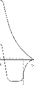 t - to= us t3-t =5us ts - to=on-period FIGURE 18.20 Ideal base current and voltage requirement of power BJT reduced by applying a negative or reverse base current instead of simply ceasing the input drive base current. Because a high-current, high-power source is required for driving the base of a power BJT, difficulty arises when the emitter is not at ground level (or at a fixed voltage). When the BJTs are connected in a bridge configuration or a load is connected between the emitter and ground, emitter terminal has a floating potential. This potential changes from zero to supply voltage and from supply voltage to zero when the BJT is switched off and switched on, respectively. Figure 18.21 shows simple base drive circuits for a power BJT. The input drive signal is amplified by a PNP transistor (Fig. 18.21a), whose ultimately drives the main power BJT. Basically, it is similar to the Darlington circuit. Figure 18.21b shows a transistor to totem-pole arrangement, which reduces power dissipation in the base drive circuit. Although this circuit operates even with unipolar dc power supply (with a 0-V rail instead of -Vqq), a negative voltage rail speeds up the turn-off transition (turn-off time reduces as in the case of MOSFET). Figure 18.21c shows a p-channel MOSFET-based driver circuit. The BJTs are driven by both unipolar as well as bipolar dc supply voltage. The emitter-to-base breakdown voltage rating (V) specifies the maximum negative rail voltage. Normally, -6 to - 8V are used. Therefore, either a ±6 or +12 and -6V rails may be selected. 18.5.5 Gate Drive Circuit for GTO The gate drive circuit (shown in Fig. 18.22) for commutation (turn-off) GTO is very similar to the transistor drive circuits discussed in the previous section. The design procedure is the same except that the antisaturation circuit (e.g., BJT in the push-pull mode) and base-to-emitter low-impedance circuit are not necessary. The gate turn-off loop (circuit) should have minimum inductance (including L), to increase reverse gate di/dt and the shorter turn-off time. Therefore, the commutation (turn-off) circuit should be fabricated as close as possible to the gate terminal of the GTO. Fiowever, with a shorter turn-off time, the turn-off gain reduces (up to unity). Therefore, the reverse commutating gate current must be almost of the same magnitude as the anode current. A high turn-off gain (over 20) can be achieved at the cost of turn-off switching losses when a slow reverse commutating gate current (slow di/dt) is apphed. 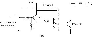 Input base dri e control si nal I I from CM S ate - Power BJ Input dri e control si nal  Power BJ 18.6 Some Practical Driver Circuits An actual drive circuit depends strongly on the type as well as the rating (power handling capability) of the power semiconductor devices. Fiowever, the basic circuit configuration does not change significantly. Figure 18.23 shows circuit diagrams for various devices. Figure 18.23a shows a Diac-based trigger circuit. Its performance is better than the previous circuit shown in Fig. 18.9. In this case an RC branch is added to make the switching angle the same in both half-cycles. Figure 18.23b shows a custom-buih IC785 used for triggering the SCR, Triac, and so forth. Figure 18.23c shows a simple driver circuit for both MOSFET and IGBT. It works satisfactorily up to several kilohertz of the switching frequency. Figure 18.23f shows a 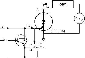 FIGURE 18.21 Base driver circuits for power BJT. FIGURE 18.22 A typical driver (commutation) circuit for GTO. Lamp Load,200W 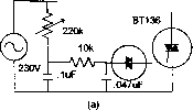 Synchronizing sinal (from ac mains, upto42V) 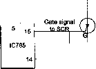 V-X Gate sinnal Gate Signal to Triac +12V Load Input gate drive control signal 1.5k 12 -ЛЛЛг- IGBT SL100 Input gate control signal л -ЛЛЛЛ On signal CSV)
О 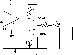 Input gate control nal  Opto-ceupter 7400 BC107 (D.(DTi I [<-I Load ~]-i I -f- (1200V,2QA) Opto-coupter (e)  -Vcc= -15V (High cunent, high power dc source) CW50DY-12H (600V.50A)
Jo.1i IR2110 IGBT power Module (Half-Bridge) FIGURE 18.23 Various practical driver circuits. custom-built driver circuit using 1С chip IR2110 for driving an IGBT power module of a half-bridge inverter circuit. Such custom-built driver circuits have high source and sink capability (2A for IR2110). References 1. B. W. Williams, Power Electronics, 2nd ed., Macmillan/ELBS, London, 1995. 2. M. H. Rashid, Power Electronics, 2nd ed., Prentice-Hall of India Pvt. Ltd., New Delhi, 1995. 3. O. P. Arora, Power Electronics Laboratory, Wheeler Publishing, Allahabad, 1993. 4. D. R. Graham and J. C. Hoy, SCR Manual, 5th ed.. General Electric, 1972. 5. Power MOSFET Transistor Data, Motorola Inc., New York, 1984. 6. B. K. Bhattacharya and S. Chatterjee, Industrial Electronics and Control, Tata-McGraw Hill Publishing Co. Ltd. New Delhi, 1995. 7. J. Ziemann and S. Grohmann, State-of-the art Power Electronics, E. P.V.Electronic-Practiker-Verlagsgesellschaft mbh, Durerstadt, 1997. 8. N. Mohan, T. M. Undeland, and W. P. Robbins, Power Electronics, 2nd ed., John Wiley & Sons (Sea), Singapore, 1995. 9. C. Licitra, S. Musumeci, A. Raciti, A.U. Galluzzo, R. Letor, and M. Melito, A new driving circuit for IGBT devices, IEEE Trans. Power Electronics 10:3, 373-378, May 1995. 10. O. H. Stile, J. J. Schulman, and J. D. Van Wok, A high-performance gate/base drive using a current source, IEEE Trans. Industry Applications 29:5, 933-939, Sept./Oct., 1993. 11. R. O. Caceresio and Ivo Barbi, A boost dc-ac converter: analysis, design, and experimentation, IEEE Trans. Power Electronics 14: (1), 134-141, Jan. 1999. 12. M. Thompson, Sizing the mosfet gate damping resistor, Newsletter of the IEEE Power Electronics Society 11:4, 2, Oct. 1999. 13. M. K. Kazimiriezuk and A. J. Edstrom, Open-Loop peak voltage feed-forward control of PWM buck converter, IEEE Trans. Circuits andn Systems-L 47:5, 740-746, May 2000. 14. S. I. Hui, S. C. Tang and H. Chung, Coreless printed circuit board transformers-fundamental characteristics and application potential, IEEE Circuits and Systems Society Newsletter 11:3, 3-15, Third Quarter 2000. Control Methods for Power Converters J. Fernando Silva, Ph.D. Instituto Superior Tecnico, CAUTL, DEEC Mdquinas Electricas e Electrdnica de Potencia (24) Technical University of Lisbon, Av. Rovisco Pais 1, 1049-001 Lisboa, Portugal 19.1 19.2 19.3 19.4 19.5 Introduction...................................................................................... 431 Power Converter Control using State-Space Averaged Models.................... 432 19.2.1 Introduction 19.2.2 State-Space Modeling 19.2.3 Converter Transfer Functions 19.2.4 Pulse Width Modulator Transfer Functions 19.2.5 Linear Feedback Design Ensuring Stability Sliding-Mode Control of Power Converters............................................ 450 19.3.1 Introduction 19.3.2 Principles of Sliding-Mode Control 19.3.3 Constant-Frequency Operation 19.3.4 Steady-state Error Elimination in Converters with Continuous Control Inputs Fuzzy Logic Control of Power Converters............................................... 481 19.4.1 Introduction 19.4.2 Fuzzy Logic Controller Synthesis Conclusions....................................................................................... 484 References.......................................................................................... 486 19.1 Introduction Electronic power converters must be suitably controlled in order to supply the voltages, currents, or frequency ranges needed for the load and to guarantee the requested dynamics. [1] Furthermore, they can be designed to serve as clean interfaces between most loads and the electrical utility system. Thereafter, the electrical utility seems to feed almost pure resistive loads. This chapter provides basic and some advanced skills to control electronic power converters, taking into account that the control of power converters is a vast and interdisciplinary subject. Control designers for power converters should know the static and dynamic behavior of the electronic power converter and how to design its elements for the intended operating modes. Designers must be experts on control techniques, especially the nonlinear ones, since power converters are nonlinear, time variant, discrete systems, and designers must be capable of analog or digital implementation of the derived modulators, regulators, or compensators. Powerful modeling methodologies and sophisticated control processes must be used to obtain stable controlled power converters not only with satisfactory static and dynamic performance, but also with low sensitivity against load or line disturbances or, preferably, robustness. In Section 19.2, techniques to obtain suitable nonlinear and linear state-space models, for most power converters, are presented and illustrated through examples. The derived linear models are used to create equivalent circuits, and to design linear feedback control methods for converters operating in the continuous or discontinuous mode. The classical linear systems control theory, based on Laplace transform, transfer function concepts. Bode plots, and root locus, is best used with state-space averaged models, or derived circuits, and the well-known triangular wave modulators for generating the switching functions or the trigger signals for the power semiconductors. Nonlinear state-space models and shding-mode controllers, presented in Section 19.3, provide a more consistent way of handling the control problem of power converters, since sliding mode is aimed at variable structure systems, as are power converters. Chattering, a characteristic of sliding mode, is inherent in switching power converters, even if they are controlled with linear methods. Chattering is very hard to remove and is acceptable in certain converter variables. The explained sliding-mode control law defines exactly the variables that need to be measured, while providing the necessary equations (control law and switching law) whose implementation gives the modulator and compensator low-level hardware (or software). Therefore, sliding-mode control integrates the design of the power converter modulator and controUer electronics, reducing the needed designer expertise. This approach requires measurement of the state variables, but ehminates conventional modulators and linear feedback compensators, enabhng better performance and robustness, whUe reducing the converter cost, control complexity, volume, and weight (the power density figure increases). The so-caUed main drawback of sliding mode, variable switching frequency, is also addressed, providing fixed-frequency auxUiary functions and suitable augmented control laws to nuU steady-state errors due to the use of constant switching frequency. Fuzzy control of power converters (Section 19.4) is a control technique needing no converter models, parameters, or operating conditions, but only an expert knowledge of the converter dynamics. Fuzzy controllers can be used in a diverse array of power converters with only smaU adaptations, since the controllers, based on fuzzy sets, are obtained simply from a knowledge of the system dynamics, using a model reference adaptive control phUosophy. Obtained fuzzy control rules can be built into a decision lookup table, in which the control processor simply picks up the control input corresponding to the sampled measurements. Fuzzy controUers are almost immune to system parameter fluctuations, since they do not take into account their values. The steps to obtain a fuzzy controller are described, and the example provided compares the fuzzy controUer performance to current mode control. 19.2 Power Converter Control using State-Space Averaged Models 19.2.1 Introduction State-space models provide a general and strong basis for dynamic modeling of various systems including power converters [6,7]. State-space models are useful to design the needed linear control loops, and can also be used to computer simulate the steady state, as weU as the dynamic behavior of the power converter, fitted with the designed feedback control loops and subjected to external perturbations. Furthermore, state-space models are the basis for applying powerful nonlinear control methods such as sliding mode. State-space averaging and linearization provides an elegant solution for the application of widely known linear control techniques to most power converters. 19.2.2 State-Space Modeling Consider a power converter with sets of power semiconductor structures, each one with two different circuit configurations, according to the state of the respective semiconductors, and operating in the continuous mode of conduction. Supposing the power semiconductors as controUed ideal switches (zero on-state voltage drops, zero off-state currents, and instanta- neous commutation between the on and off states), the time (t) behavior of the circuit, over period T, can be represented by the general form of the state-space model (19.1): X = Ax + Bu у = Cx + Du (19.1) where x is the state vector, x = dx/dt, u the input or control vector, and A, B, C, D are respectively the dynamics (or state), the input, the output and the direct transmission (or feedforward) matrices. Since the power semiconductors wiU either be conducting or blocking, the time-dependent switching function 3(t) can be used to describe the aUowed switch states of each structure (e.g., S(t) = 1 for the on state circuit and S(t) = 0 for the off state circuit). Then, two subintervals must be considered: subinterval 1 for 0 < t < T, where S(t) = 1 and subinterval 2 for iT < t < T where S(t) = 0. The state equations of the circuit, in each of the circuit configurations, can be written as: X = AjX + BjU у = Qx + Diu X = A2X + B2U у = C2X + D2U for 0 < t < 1T where S(t) = 1 (19.2a) for 1T < t < T where 3(t) = 0 (19.2b) 19.2.2.1 Switched State-Space Model Given the two binary values of the switching function 3(t), (19.2a) and (19.2b) can be combined to obtain the nonlinear and time-variant switched state-space model of the power converter circuit, (19.3) or (19.4): X = [AiS(t) + A2(l - S(t)]x + [BiS(t) + B2(l - S(mu у = [CiS(t) + €2(1 - S(mx + [DiS(t) + D2(l - smu (19.3) X = A5X + B5U у = C5X + D5U (19.4) where As С [AiS(t) + A2(l-Sm [Bi + B2(l-(T))] [Ci + C2(l-(T))] Ds = [DiS(t)D2(l-Sm. 19.2.2.2 State-Space Averaged Model Since the state variables of the x vector are continuous, using (19.3), with the initial conditions Xi(0) = X2(T), X2(iT) = Xi(diT), and considering the duty cycle as the average value of (t), the time evolution of the converter state variables can be obtained, integrating (19.3) over the intervals 1 ... 40 41 42 43 44 45 46 ... 91 |
|||||||||||||||||||||||||||||||||||||||||||||||||||
|
© 2026 AutoElektrix.ru
Частичное копирование материалов разрешено при условии активной ссылки |