 |
 |
 |
| Главная Журналы Популярное Audi - почему их так назвали? Как появилась марка Bmw? Откуда появился Lexus? Достижения и устремления Mercedes-Benz Первые модели Chevrolet Электромобиль Nissan Leaf |
Главная » Журналы » Metal oxide semiconductor 1 ... 41 42 43 44 45 46 47 ... 91 0 < t < diT and SiT < t < T, although it often requires excessive calculation effort. However, a convenient approximation can be devised, considering 1 the maximum of the absolute values of all eigenvalues of A (usually 1 is related to the cutoff frequency of an equivalent low-pass filter with < l/T). For Ajnax < 1 the exponential matrix (or state transition matrix) e = I + At + At/2 H-----h A /: /n!, where I is the identity or unity matrix, can be approximated by e I + At. Therefore, a,S,tMl-S,)t I [д^ Fience, the solution over the period T, for the system represented by (19.3), is found to be: x(T) e[ii+2-i]Xi(0) g[A,,+A,(l-0](T-T)[B + B2(l - i)]udT (19.5) This approximate response of (19.3) is identical to the exact response obtained from the nonlinear continuous time invariant state space model (19.6), supposing that the average values of x, denoted x, are the new state variables, and considering 2 = 1 ~ i- Moreover, if A A2 = A2 A the approximation is exact. X = [Aii + A22]x + [Bii + B22]u у = [Cii + C22]x + [Dii + D22]u (19.6) For Я^д^Т 1, the most often referred to as the state space averaged model (19.6), is also said to be obtained by averaging (19.3) over one period, under small ripple and slow variations, as the average of products is approximated by products of the averages. By comparing (19.6) to (19.1), the relations (19.7), defining the state-space averaged model, are obtained. A = [Aii+A22]; c = [Cii + C22]; B = [Bii + B22]; D = [Dii+D22]. (19.7) The differential equations governing the dynamics of the state vector x = [i, vj С denotes the transpose of vectors or matrices) are: r - E± Ql is on and is off) (19.8a) iorSiT <t < T(S(t) = 0, dv . v Q is off and D, is on) (19.8b) Comparing (19.8) to (19.2) and considering у = [v, ij the following matrices can be identified: 0 -l/(R,C,) ; A2 = 0 -l/L; 1/Q -l/(i? Q B, =[l/L 0f;B2 = [0,0f;u = [Voc];
; Dl = [0, 0]; D2 = [0, 0] From (19.3) and (19.4), the switched state space model of this power converter is: 0 -(1 - 3it))/L, 1(1-S(T))/C, -l/(R,CJ JLfJ m/Li
(19.9) Example 19.1. State-Space Models for the Buck-Boost dc/dc Converter. Consider the simplified circuitry of the buck-boost converter of Fig. 19.1 switching at f, = 20 kHz (T = 50 s) with Vocmax = 28 V, DCmin = 22 V, V, = 24 V, Ц = 400 цН, 2700 iF, i? = 2 Q. С >R,.
FIGURE 19.1 (a) Basic circuit of the buck-boost dc/dc converter; (b) ideal waveforms. Now applying (19.6), Eqs. (19.10a) and (19.10b) can be obtained: L J 0 0 -1 RoCo.
[Vdc] (19.10a) (19.10b) From (19.10), the state space averaged model, written as function of is: 1-1 -1
(19.11a) (19.11b) The eigenvalues 5 , or characteristic roots of A, are the roots of I si - A. Therefore: (l-l) 2R,C, 4(R,C,y ЦС, (19.12) Since Ajnax is the maximum of the absolute values of aU the eigenvalues of A, the model (19.11) is valid for switching frequencies = 1/T) that verif) max 1- Therefore, as T Vmax the values of T that approximately verif) this restriction are T l/max(5 J). Given this buck-boost converter data, T 2 ms is obtained. Therefore, the converter switching frequency must obey max(5y- ), implying switching frequencies above, say, 5 kHz. Consequently, the buck-boost switching frequency, the inductor value and the capacitor value, were chosen accordingly. This restriction can be further used to discuss the maximum frequency ш^ах for which the state-space averaged model is still valid, given a certain switching frequency. As X- can be regarded as a frequency, the preceding constraint brings (o 2я, say, (o < InfJlOy which means that the state-space averaged model is a good approximation at frequencies under one tenth of the power converter switching frequency. FIGURE 19.2 Equivalent circuit of the averaged state-space model of the buck-boost converter. The state-space averaged model (19.11) is also the state-space model of the circuit represented in Fig. 19.2. Hence, this circuit is designated as the averaged equivalent circuit of the buck-boost converter and aUows the determination, under smaU ripple and slow variations, of the average equivalent circuit of the converter switching ceU (power transistor plus diode). The average equivalent circuit of the switching ceU (Fig. 19.3a) is represented in Fig. 19.3b and emerges directly from the state space averaged model (19.11). This equivalent circuit can be viewed as the model of an ideal transformer (Fig. 19.3c), whose primary to secondary ratio (11/12) be calculated applying Kirchhoff voltage laws to obtain -Vi-\-v - V2 = 0.Ks V2 = SiV, it follows that Vi = v(l - 3i), giving (V1/V2) = (1 - The same ratio could be obtained beginning with = ц + /2, and ц = Sii (Fig. 19.3b), which gives /2 = hi - 1) and (/2/*1) = 2/1- The average equivalent circuit concept, obtained from (19.6) or (19.11), can be applied to other power converters, with or without a similar switching cell, to obtain transfer functions or to computer simulate the converter average behavior. The average equivalent circuit of the switching ceU can be applied to converters with the same switching ceU operating in the continuous conduction mode. However, note that the state variables of (19.6) or (19.11) are mean values of the converter instantaneous variables and, therefore, do not represent their ripple components. The inputs of the state-space averaged model are the mean values of the inputs over one switching period. D.  FIGURE 19.3 Average equivalent circuit of the switching cell, (a) Switching cell; (b); average equivalent circuit; (c) average equivalent circuit using an ideal transformer. 19.2.2.3 Linearized State-Space Averaged Model Since the converter outputs у must be regulated actuating on the duty cycle 3(t), and the converter inputs u usually present perturbations due to load and power supply variations, state variables are decomposed in small ac perturbations (denoted by ~ ) and dc steady-state quantities (represented by uppercase letters). Therefore: X = X + x y = Y + y u = U + u Si=AiS 32 = A2-3 (19.13) Using (19.13) in (19.6) and rearranging terms, we obtain i = [AiZli + A2Zl2]X+ [BiZli +B2Zl2]U + [AlZli + A2Zl2]x + [(Al - A2)X + (Bl - В2МЗ + [BiZli + B2Zl2]u + [(Al - A2)x + (Bl - В2)й]3 (19.14) Y + y = [CiZli +C2Zl2]X+[DiZli +D2Zl2]U + [CiZli + C2Zl2]x + [(Ci - C2)X + (Dl - D2M3 + [DiZli + D2Zl2]u + [(Ci - C2)x + (Dl - D2)u] (19.15) The terms [AiZli +A2Zl2]X+[BiZli +B2Zl2]U [CiZli + C2Zl2]X + [DiZli + D2Zl2]U, respectively from (19.14) and from (19.15), represent the steady-state behavior of the system. As in steady state X = 0, the following relationships hold: 0 = [AiZli +A2Zl2]X + [BiZli +B2Zl2]U (19.16) Y = [CiZli + C2Zl2]X + [DiZli + D2Zl2]U (19.17) Neglecting higher order terms ([Ai - A2)x + (Bi - B2)u] 0) of (19.14) and (19.15), the linearized small-signal state-space averaged model is: к = [AiZli + A2A2]x + [(Al - A2)X + (Bl - B2)U] + [BiZli +B2Zl2]U У = [CiZli + C2A2]x + [(Ci - C2)X + (Dl - D2M3 + [DiZli +D2Zl2]u (19.19) X = A x + B u + [(Al - A2)X + (Bl - B2)U] у = + D u + [(Ci - C2)X + (Dl - D2M3 with: A = [AiZli+A2Zl2] B = [BiZli+B2Zl2] C = [CiZli+C2Zl2] D = [DiZli+D2Zl2] 19.2.3 Converter Transfer Functions Using (19.16) in (19.17) the input U to output Y steady state relations (19.21), needed for open-loop and feed-forward control, can be obtained: (19.20) (19.21) Applying Laplace transforms to (19.19) with zero initial conditions, and using the superposition theorem, the small signal duty-cycle 3 to output у transfer functions (19.22) can be obtained considering zero hne perturbations {й = 0). fis). ~S(s) = CJsl - A,J-[(Ai - A2)X + (Bl - B2)U] + [(Ci-C2)X+(Di-D2)U] (19.22) The hne to output transfer function (or audio susceptibihty transfer function) (19.23) is derived using the same method, considering now zero small signal duty-cycle perturbations Cs = 0). u(s) = Cj5l-AJ-B + D, (19.23) Example 19.2. Buck-boost dc/dc Converter Transfer Functions. From (19.11) of Example 19.1 and (19.19), making X = [4, У/, YlV.jJ and и - [VqcIj the linearized state space model of the
[vdc] ё 4 0. Li 0
(19.24a) From (19.20) and (19.24) the following matrices are identified: av - ц (19.24b) The averaged linear equivalent circuit, resulting from (19.24a) or from the linearization of the averaged equivalent circuit (Fig. 19.2) derived from (19.11), now includes the smaU signal current source 3li in parallel with the current source Ai, and the small signal voltage source S(Vjq + V) in series with the voltage source Ai(vp)c + o)- The supply voltage source Vjc is replaced by the voltage source й^) Using (19.24b) in (19.21), the input U to output Y steady-state relations are: (19.25a) (19.25b) Vq A, Vdc 1-1 These relations are the known steady-state transfer relationships of the buck-boost converter [13]. For open-loop control of the output, knowing the nominal value of the power supply V the required V, the value of A can be off-line calculated from (19.25b) (Zli = VoliVo + Vbc))- A modulator such as that described in Section 19.2A, with the modulation signal proportional to A, would generate the signal d(t). Open-loop control for fixed output voltages is possible. A,(lsCM Vdc(s) s4iC,R, + sLi + R(l - A Vo(s) R,A,(l-A,) vnc(s) s4,C,R, + sL, + R,(l-A,f (19.26a) (19.26b) From (19.22), the small-signal duty-cycle S to output у transfer functions are: \(s) Dc(l + 1 + sW/( -A,) 3(s) s4,C,R, + sL, + RXl-A,f io(s) VDc(Ro-sL,A,/(l-A,f) 3(s) s4,C,R, + SL, + RXl-A,f (19.27a) (19.27b) These transfer functions enable the choice and feedback loop design of the compensation network. Note the positive zero in vXs)/d(s), pointing out a nonmini-mum-phase system. These equations could also be obtained using the small signal equivalent circuit derived from (19.24), or from the linearized model of the switching ceU (Fig. 19.3.b), substituting the current source Sii by the current sources Ai and SI in parallel, and the voltage source Sv by the voltage sources Ai(vp)c + v) and (Vc + o) i series. Example 19.3. Transfer Functions of the Forward dc-dc Converter. Consider the forward (buck-derived) converter of Fig. 19.4 switching at /, = 100 kHz (T = 10 is) with Vp)c = 300 V, п = 30, = 5 V, Ц = 20 iH, Vl = 0.01 Q, C, = 2200 iF, Гс = 0.005 Q, i = 0.lQ. Assuming X = [i, Vq], 3(t) = I when both Q, are on and D2 is off (0 < t < T), S(t) = 0 when both Ql, Dl are off and d2 is on ( T < t < T), the switched if the power supply V is almost constant and the converter load does not change significantly. If the V value presents disturbances, then feed-forward control can be used, calculating A on-hne, so that its value will always be in accordance with (19.25b). The correct value wiU be attained at steady state, despite input voltage variations. However, because of converter parasitic reactances, not modeled here (see Example 19.3), in practice a steady-state error would appear. Moreover, the transient dynamics imposed by the converter would present overshoots, being often not suited for demanding apphcations. From (19.23), the line to output transfer functions are: buck-boost converter is: 0  D n
2T t a) b) FIGURE 19.4 (a) Basic circuit of the forward dc-dc converter; (b) circuit main waveforms. state-space model of the forward converter, considering as output vector у = [г^, v, is: di, {Rjc + КЧ + Vc), dt Ц{К, + Гс) Ro , -5(0 с L,iRo + Rc) R. Vc + - (19.28) dt (R, + Гс)С, (R, + Гс)С, Vr . 1 l + rc/i?/l + rc/i? Making = гс/(1 + R , = R + rc. Kc = Rq/Roc = + cm comparing (19.28) to (19.2), the following matrices can be identified: -Гр/Ц -kJLi kJC, -1/(R C,) Bl = [l/( a of; B2 = [0, of; u = [Уос] 1 0 ;Di =D2 =[0, Of Ci = = cm oc Now, applying (19.6), the exact (since = A2) state-space averaged model (19.29) is obtained: -гр/ц -Кс/Ц
[Vdc] (19.29a) [Vocl (19.29b) Since Al - A2, this model is valid for (o < 2nf. The converter eingenvalues Sf are:
Rocfio The equivalent circuit arising from (19.29) is represented in Fig. 19.5. It could also be obtained with the concept of the switching cell equivalent circuit (Fig. 19.3 of Example 19.1). Making X = [4, Vcf, Y = [4, Vf and U = [V cl from (19.19) the small-signal state-space averaged model is: -гр/ц -КсШ lc j
[3] (19.31a) [vr,c] (19.31b) From (19.21) the input U to output Y steady-state relations are:
Vdc п(к1Лс + гр) V, A,(kiR + r,j Vdc n(kiR + Гр) (19.32a) (19.32b) Making Гс = 0, = 0 and /7 = 1, the former relations give the well-known dc transfer relationships of the buck dc-dc converter. Relations (19.32) allow the open-loop and feed-forward control of the converter, as discussed in Example 19.2, provided that all the modeled parameters are time invariant and accurate enough.  FIGURE 19.5 Equivalent circuit of the averaged state-space model of the forward converter. From (19.23) the line to output transfer functions are derived: lis) 1(1 vr)c(s) s4,C,R + sm + C,R,jp) + klR + Гр (19.33a) ~ -rilcRoc + cm + oRoJcm) ?,C() ~ A-Qac + + Qi rp) + /C2,i + Tp (19.33b) Using (19.22), the smaU-signal duty cycle д to output у transfer functions are: (1 + sC,Rj lis) (5) s4,C,R + sm + C,R,jp) + kiR + Гр (19.34a) (klcRoc + cm + SCRJ) (5) s4,C,R + 5(L, + C,i rp) + kiR + Гр (19.34b) The real zero of (19.34b) is due to r, the equivalent series resistance (ESR) of the output capacitor. A similar zero would occur in the buck-boost converter (Example 19.2), if the ESR of the output capacitor was included in the modehng. 19.2.4 Pulse Width Modulator Transfer Functions In what is often referred to as pulse width modulation (PWM) voltage mode control, the output voltage u(t) of the error (between desired and actual output) amplifier plus regulator. processed if needed, is compared to a repetitive or carrier waveform r(t), to obtain the switching function 3(t) (Fig. 19.6a). This function controls the power switch, turning it on at the beginning of the period and turning it off when the ramp exceeds the u(t) voltage. In Fig. 19.6b the opposite occurs (turn-off at the end of the period, turn-on when the u(t) voltage exceeds the ramp). Considering r(t) as represented in Fig. 19.6a (r(t) = urnj/T\ is obtained equating r{t) = щ giving = u,(t)/u, or SJu,(t) = Gm (Gm = l/u,J. In Fig. 19.6b the switching-on angle a is obtained from giving ccj, = (я/2) X (1 - w,/w,max) and = дсс^дщ = -/(2wjaJ. Since, after turn-off or turn-on, any control action variation of u(t) will only affect the converter duty cycle in the next period, a time delay is introduced in the control loop. For simplicity, with smaU signal perturbations around the operating point, this delay is assumed almost constant and equal to its mean value (T/2). Then, the transfer function of the PWM modulator is: ks) -sT/2 T s {ту {TV (19.35) The final approximation of (19.35), valid for шТ/2 < a/2/2, [2] suggests that the PWM modulator can be considered as an amplifier with gain Gm and a dominant pole. Notice that this pole occurs at a frequency doubling the switching frequency, and most state-space averaged models are valid only for frequencies below one-tenth of the switching frequency. Therefore, in most situations this modulator pole can be neglected, being simply (5) = u(s\ as the dominant AT t -(5(0 Ucmax 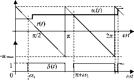 \ T I 2Г I 3T \ 4T t 5jT T+52T 2Т+5зТ ЗТ+54Т a) r(t)=Ucn,ax tIT b) r(t)=Ucn,ax-2Ucn,axCOt/7z FIGURE 19.6 Waveforms of pulse width modulators showing the variable time delays of the modulator response. pole of (19.35) stays, at least one decade to the left of the dominant poles of the converter. 19.2.5 Linear Feedback Design Ensuring Stability In the apphcation of classical linear feedback control to power converters. Bode plots and root-locus are usually suitable methods to assess system performance and stability. General rules for the design of the compensated open-loop transfer function are as follows: (i) The low-frequency gain should be high enough to minimize output steady-state errors. (ii) The frequency of 0 dB gain (unity gain), ш^, should be placed close to the maximum allowed by the modeling approximations (Я^ !) practice, this frequency should be almost an order of magnitude lower than the switching frequency. (iii) To ensure stability, the phase margin, defined as the additional phase shift needed to render the system unstable without gain changes (or the difference between the open loop system phase at cOqj and - 180°) must be positive, and in general greater than 30° (45°-70° is desirable). In the root locus, no poles should enter the right half of the complex plane. (iv) To increase stability, at the frequency where the phase reaches -180°, the gain should be less than -30 dB (gain margin greater than 30 dB). Transient behavior and stabihty margins are related: The obtained damping factor is generally 0.01 times the phase margin (in degrees), and overshoot (in percent) is given approximately by 75° minus the phase margin. The product of the rise time (in seconds) and the closed loop bandwidth (in rad/s) is close to 2.8. To guarantee gain and phase margins the following series compensation transfer functions (usually implemented with operational amplifiers) are often used. 19.2.5.1 Lag or Lead Compensation Lag compensation should be used in converters with good stabihty margin but poor steady state accuracy. If the frequencies 1/T and 1/T ((19.36) with 1/T < 1/TJ are chosen well below the unity gain frequency, lag-lead compensation lowers the loop gain at high frequency but maintains the phase unchanged for ш 1 / T. Then, the dc gain can be increased to reduce the steady-state error without significantly decreasing the phase margin. 1 + 5T, TAs+l/T. (19.36) Lead compensation can be used in converters with good steady-state accuracy but poor stability margin. If the frequen- cies 1/T and 1/T ((19.36) with 1/T > 1/TJ are chosen below the unity gain frequency, lead-lag compensation increases the phase margin without significantly affecting the steady-state error. The Tp and values are chosen to increase the phase margin, fastening the transient response and increasing the bandwidth. 19.2.5.2 Proportional-Integral Compensation Proportional-integral (PI) compensators (19.37) are used to guarantee null steady-state error with acceptable rise times. PI compensators are a particular case of lag-lead compensators, therefore suitable for converters with good stability margin but poor steady-state accuracy. , , lsT, T, 1 Tp sTp i + - 1 + . (19.37) 19.2.5.3 Proportional-Integral plus High-Frequency Pole Compensation This integral plus zero-pole compensation (19.38) combines the advantages of a PI with lead or lag compensation. Can be used in converters with good stability margin but poor steady-state accuracy. If the frequencies 1/T and 1/T (1/T < 1/T) are carefully chosen, compensation lowers the loop gain at high frequency, while only slightly lowering the phase to achieve the desired phase margin. 1+5T, 5Т^(1+5Тм) 5 + 5+ l/T, Т,Тм 5(5+1/Тм) 5(5+ Шм) (19.38) 19.2.5.4 Proportional Integral Derivative (PID), plus High-Frequency Poles The PID notch filter type (19.39a) scheme is used in converters with two lightly damped complex poles, to increase the response speed, while ensuring zero steady-state error. In most power converters, the two complex zeros are selected to have a damping factor greater than the converter complex poles, but on oscillating frequency that is slightly smaller. The high-frequency pole is placed to achieve the needed phase margin. The design is correct if the complex pole loci, heading to the Modulator FIGURE 19.7 Block diagram of the linearized model of the closed loop buck-boost converter. complex zeros in the system root locus, never enter the right half-plane. PIDnf(s) - + 2(,рШо,р5 + col 5(1 + s/CDpi) 1 + s/(Dpi 1 + s/(Dpi 5(1 + s/CDpi) 1 +5/Ш cpOcp(l + Ыср/<Оср) 5(1 + S/Copi) (19.39a) For systems with a high frequency zero placed at least one decade above the two lightly damped complex poles, the compensator (19.39b), with coi < py be used. Usually, the two real zeros present frequencies slightly lower than the frequency of the converter complex poles. The two high frequency poles are placed to obtain the desired phase margin [4]. The obtained overaU performance wiU be inferior to that of the PID type notch fiber. Cpid(s) = (1 + 5/ш,1)(1 + 5/ш,2) 5(1 + S/C0,f (19.39b) Example 19.4. Feedback Design for the Buck-Boost dc-dc Converter. Consider the converter output voltage (Fig. 19.1) to be the controlled output. From Example 19.2 (19.26b) and (19.27b), the block diagram of Fig. 19.7 is obtained. The modulator transfer function is considered a pure gain (G = 0.1). The magnitude and phase of the open loop transfer function v/u (Fig. 19.8a) traces 1), shows a resonant peak due to the two lightly damped complex poles and the associated -12 dB/octave roll-off. The right half-plane zero changes the roU-off to -6 dB/octave and adds -90° to the converter phase (nonminimum phase converter). The procedure to select the compensator and to design its parameters can be outlined as foUows: 1. Compensator selection. Since V perturbations exist, nuU steady-state error guarantee is needed. High-frequency poles are usually needed, given the -6 dB/octave final slope of the transfer function. Therefore, two ((19.38) and (19.39a)) compensation schemes with integral action can be tried. Compensator (19.39a) is usually convenient for systems with lightly damped complex poles. Buck-Boost converter, PI plus high frequency pole 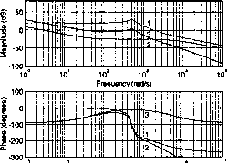 10= 10 Frequency (rad/fe) Buck-Boost converter, PD notch filter 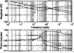 10= 10 Frequency (rad) FIGURE 19.8 Bode plots for the buck-boost converter. Trace 1, power converter magnitude and phase; trace 2, compensator magnitude and phase; trace 3, resulting magnitude and phase of the compensated converter, (a) pi plus high-frequency pole compensation with 30° phase margin, coqj = 50rad/s, selected W = 300rad/s, cn = 45rad/s, = 45rad/s; (b) 0.083 rad,r,Xo pid notch filter 40.2 rad/s, compensation 12900 rad/s. with 64° phase margin, 2. Unity gain frequency cOq choice: If the selected compensator has no complex zeros, it is better to be conservative choosing odB 11 below the frequency of the converter hghtly damped poles. However, because of the resonant peak of the converter transfer function, the phase margin can be obtained at a frequency near the resonance. If the phase margin is not enough, the compensator gain must be lowered. If the selected compensator has complex zeros, (Dqb be chosen slightly above the frequency of the lightly damped poles. 3. Desired phase margin (фм) specification ф^ > 30° (preferably between 45° and 70°). 4. Compensator pole zero placement to achieve the desired phase margin: With the integral plus zero-pole compensation (19.38), the compensator phase ф^р, at the maximum frequency of unity gain (often cOqj), equals the phase margin (ф^) minus 180° and minus the converter phase ф^, (ф^р = - 180° - ф^). The zero-pole position can be obtained calculating the factor fct = tg(7r/2 + ф,р/2) being = а)в а and . In the PID notch filter (19.29a), the two complex zeros are placed to have a damping factor equal to two times the damping of the converter complex poles, and oscillating frequency Шдр 30% smaller. The high-frequency pole CDpi is placed to achieve the needed phase margin (ш^ (ш, with /J = tg(7i/2 + and ф^ = Фм- 180° - ф ) [10]. 3-60 0.005 0.01 0.015 0.02 0.025 0.03 0.035 0.04 t[sl I- 0 0.005 0.01 0.015 0.02 t[s] 0.025 0.03 0.035 0.04 5. Needed compensator gain calculation (the product of the converter and compensator gains at the cDqb frequency must be 1). 6. Stability margins verification using Bode plots and root locus. 7. Results evaluation. Restarting the compensator selection and design, if the attained results are not suitable. The buck-boost converter controlled with integral plus zero-pole compensation presents, in closed loop, two complex poles closer to the imaginary axes than in open-loop. These poles should not dominate the converter dynamics. Instead, the real pole resulting from the open-loop pole placed at the origin should be almost the dominant one, thus slightly lowering the calculated compensator gain. If the cOqb frequency is chosen too low, the integral plus zero-pole compensation turns into a pure integral compensator (ш, = ш^ = cDqb)-However, the obtained gains are too low, leading to very slow transient responses. Resuhs showing the transient responses to vf and V]c step changes, using the selected compensators (Fig. 19.8) are shown (Fig. 19.9). The compensated real converter transient behavior occurs in the buck and in the boost regions. Notice the nonminimum phase behavior of the converter (mainly in Fig. 19.9b), the superior performance of the PID notch filter compensator, and the unacceptable behavior of the PI with high-frequency pole. Care should be taken with load changes, when using this compensator, since instability can easily occur. The compensator critical values, obtained with root-locus studies, are Wp = 700 for the integral plus zero-pole compensator, TpnY = 0.0012 for the PID notch filter, and Wjp = 18, for the integral compensation derived from the integral plus zero-pole compensator 0 0.005 0.01 0.015 0.02 0.025 0.03 0.035 0.04 t[s] 3*60 0.005 0.01 0.015 0.02 t[s] 0.025 0.03 0.035 0.04 FIGURE 19.9 Transient responses of the compensated buck-boost converter. At = 0.005 s yj step from 23 V to 26 V. At = 0.02 s Vf)( step from 26 V to 23 V. Top graphs: square reference vjj- and output voltage v. Bottom graphs: traces around 20, current; traces starting at zero, 10 X (vjj- - Vq). (a) PI plus high-frequency pole compensation with 60° phase margin and coqj = 500 rad/s; (b) PID notch filter compensation with 64° phase margin and coqj = 1000 rad/s. oref Modulator ► ОС cm + *6> Roccm ) FIGURE 19.10 Block diagram of the linearized model of the closed-loop controlled forward converter. (ш^ = Шм). This confirms the Bode plot design and aUows stability estimation with changing loads and power supply. Example 19.5. Feedback Design for the Forward dc/dc Converter. Consider the output voltage of the forward converter (Fig. 19.4a) to be the controlled output. From Example 19.3 (19.33b) and (19.34b), the block diagram of Fig. 19.10 is obtained. As in Example 19.4, the modulator transfer function is considered a pure gain (G = 0.1). The magnitude and phase of the open-loop transfer function (Fig. 19.11a, trace 1) shows an open-loop stable system. Since integral action is needed to have some disturbance rejection of the vohage source Vj)q, the compensation schemes used in Example 19.4, obtained using the same procedure (Fig. 19.11), were also tested. Results, showing the transient responses to vf and Vdc step changes, are shown (Fig. 19.12). Both compensators ((19.38) and (19.39a)) are easier to design than the ones for the buck-boost converter, and both have acceptable performances. Moreover, the PID notch filter presents a much faster response. Alternatively, a PID feedback controUer such as (19.39b) can be easily hand adjusted, starting with the proportional, integral, and derivative gains aU set to zero. In the first step, the proportional gain is increased untU the output presents an osciUatory response with nearly 50% overshoot. Next, the derivative gain is slowly increased untU the overshoot is eliminated. Lastly, the integral gain is increased to eliminate the steady-state error as quickly as possible. Example 19.6. Feedback Design for Phase-controlled rectifiers in the continuous mode. Phase controlled, p pulse (p > 1), thyristor rectifiers (Fig. 19.13a), operating in the continuous mode, present an output voltage with p identical segments within the mains period T. Given this cyclic waveform, the A, B, C, and D matrices for aU these p intervals can be written with the same form, in spite of the topological variation. Hence, the state-space averaged model is obtained simply by averaging aU the variables within period Forward coTTverter, PI plus Ngh frequerx:y pole 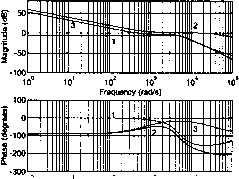 -300 Forward converter, PD notch filter 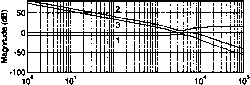 10* 10 Frequency (rad/s)  10 10 10 10 10 10 10 10 Frequency (rad/s) Frequency (rad/s) a) b) FIGURE 19.11 Bode plots for the forward converter. Trace 1, power converter magnitude and phase; trace 2, compensator magnitude and phase; trace 3, resulting magnitude and phase of the compensated converter, (a) pi plus high-frequency pole compensation with 115° phase margin, cooj5 = 500 rad/s and calculated = 36,000 rad/s, = 770 rad/s, = 30,600 rad/s; (b) pid notch filter compensation with 85° phase margin, = 6000rad/s and selected Tp 0.001 s, 2Г^Сф 1.9rad, TpOjlp - 10,000rad/s, Wp 600rad/s. 1 ... 41 42 43 44 45 46 47 ... 91 |
||||||||||||||||||||||||||||||||||||||||||||||||||||||||||||||||||||||||||||||||||||||||||||||||||||||||||||||||||||||||||||||||||||||||||||||||||||||||||||||||||||||||||||||||||||||||||||||||||||||||||||||||||||||||||||||
|
© 2026 AutoElektrix.ru
Частичное копирование материалов разрешено при условии активной ссылки |