 |
 |
 |
| Главная Журналы Популярное Audi - почему их так назвали? Как появилась марка Bmw? Откуда появился Lexus? Достижения и устремления Mercedes-Benz Первые модели Chevrolet Электромобиль Nissan Leaf |
Главная » Журналы » Metal oxide semiconductor 1 ... 42 43 44 45 46 47 48 ... 91 I 20 0.005 0.01 tis] 0.015 0.02 0.005 0.01 t[s] 0.015 0.02 i40 120 Ь 0 & 0 0.005 0.005 0.01 t[sl 0.01 t[s] 0.015 0.02 0.015 0.02 FIGURE 19.12 Transient responses of the compensated forward converter. At = 0.005 s vjj- step from 4.5 V to 5 V. At = 0.01 s F- step from 300 V to 260 V. Top graphs: square reference yref output voltage v. Bottom graphs: top traces current; bottom traces 10 x (vj-f - v). (a) PI plus high-frequency pole compensation with 115° phase margin and coqj = 500 rad/s; (b) PID notch filter compensation with 85° phase margin and odB = 6000 rad/s. T/p. Assuming small variations, the mean value of the rectifier output voltage Ujq can be written [8]: DC = () (19.40) where a is the triggering angle of the thyristors, and Up the maximum peak value of the rectifier output voltage, determined by the rectifier topology and the ac supply voltage. The a value can be obtained (a = (я/2) x (1 - w/wmax)) using the modulator of Fig. 19.6b, where со = 2n/T is the mains frequency. From (19.40), the incremental gain of the modulator plus rectifier yields: TIU, 2Wcmax (19.41) For a given rectifier, this gain depends on and should be calculated for a certain quiescent point. Fiowever, for feedback design purposes, keeping in mind that the rectifier could be required to be stable in all operating points, the maximum value of K, denoted K, can be used: sm - X max \P (19.42) The operation of the modulator, coupled to the rectifier thyristors, introduces a time delay, with mean value T/2p. Therefore, from (19.35) the modulator-rectifier transfer function Gp{s) is: uAs) p-5(T/2p) (19.43) Considering zero Up perturbations, the rectifier equivalent averaged circuit (Fig. 19.13b) includes the loss-free rectifier output resistance due to the overlap in the commutation phenomenon caused by the mains inductance [8,14]. Usually, Rl pcol/n where / is the equiva- ref + Modulator ac mams p pulse, phase controlled rectifier  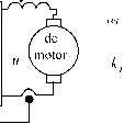 ps \-\ )k и и a) b) FIGURE 19.13 (a) Block diagram of гр pulse phase controlled rectifier feeding a separately excited dc motor, (b) Equivalent averaged circuit. lent inductance of the lines paraUeled during the overlap, half the equivalent line inductance for most rectifiers, except for single-phase bridge rectifiers where / is the line inductance. is the smoothing reactor and R, L, and are respectively the armature internal resistance, inductance, and back electromotive force of a separately excited dc motor (typical load). Assuming the mean value of the output current as the controlled output, making = + L, R, = R, + Rm, T, = LJR and applying Laplace transforms to the differential equation obtained from the circuit of Fig. 19.13b, the output current transfer function is: Ucis) - EXs) i,(l + sT,) (19.44) The rectifier and load are now represented by a perturbed (£) second-order system (Fig. 19.14). To achieve zero steady-state error, which ensures steady state insensitivity to the perturbations, and to obtain closed-loop second-order dynamics, a PI controUer (19.37) was selected for Cp{s) (Fig. 19.14). Canceling the load pole (-l/T) with the PI zero (-1/TJ yields: (19.45) The rectifier closed-loop transfer function io(s)/ioref() with zero E perturbations, is: IpKpMRJpT) io(s) i ,f(s) 52 + (2p/T)s + 2pKpMk/(RJpT) (19.46) The final value theorem enables the verification of the zero steady-state error. Comparing the denominator of (19.46) to the second-order polynomial 5 + 2Сш 5 + (dI yields: col = 2pKpMkj/(RJpT) AcdI = (2p/Tf (19.47) Since only one degree of freedom is avaUable (T), the damping factor С is imposed. Usually С = V2/2 is selected, since it often gives the best compromise between response speed and overshoot. Therefore, from (19.47), (19.48) arises: Tp = 4i:KpMkiT/(2pR,) = KpMkT/ipR,) (19.48) К и 1 + 5- DCJ. 1 Note that both (19.45) and Tp (19.48) are dependent upon circuit parameters. They wiU have the correct values-only for dc motors with parameters closed to the nominal load value. Using (19.48) in (19.46) yields (19.49), the second-order closed-loop transfer function of the rectifier, showing that, with loads close to the nominal value, the rectifier dynamics depend only on the mean delay time T/2p. ioref(s) 2(T/2p)52+5T/p+l (19.49) FIGURE 19.14 Block diagram of a PI controlled p pulse rectifier. From (19.49) ш„ = л/2р/Т results, which is the maximum frequency aUowed by соТ/2р < a/2/2, the validity limit of (19.43). This imphes that С > V2/2, which confirms the preceding choice. For Up = 310 V, p = 6, T = 20 ms, / = 0.8 mH, R = 0.5 Q, Ц = 50 mH, E = -150 V, u, = 10 V, kj = 0.1, Fig. 19.15a shows the rectifier output voltage un(on = o/p) and the step response of the output current ijv, (ijv = i/40) in accordance with (19.49). Notice that the rectifier is operating in the inverter mode. Figure 19.15b shows the effect, in the current, of a 50% reduction in the E value. The output current is initially disturbed but the error vanishes rapidly with time. This modeling and compensator design are vahd for smaU perturbations. For large perturbations either the rectifier wiU saturate or the firing angles wiU originate large current overshoots. For large signals, antiwindup schemes (Fig. 19.16a) or error ramp limiters (or soft starters) and hmiters of the PI integral component (Fig. 19.16b) must be used. These solutions wiU also work with other power converters. To use this rectifier current controUer as the inner control loop of a cascaded controUer for the dc motor speed regulation, a useful first-order approximation of (19.49) is io(s)/ioref(s) l/(5T/p+ 1). Although aUowing a straightforward compensator selection and precise calculation of its parameters, the rectifier modeling presented here is not suited for StabUity studies. The rectifier root locus wiU contain two complex conjugate poles in branches paraUel to the imaginary axis. To study the current controUer stabUity, at least the second-order term of (19.43) is needed. Alternative ways include -sT/2p sT/4p)/(l + 5T/4P), the first-order Fade approximation of q~/P or the second-order approximation, -sT/ip ip (5T/2p)Vl2)/(l + 5T/4p + (5T/2p)Vl2). 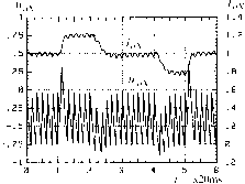 .25 r -.25 -.5 -.75 -1 ......................- 1.2 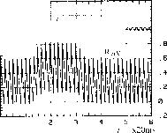 FIGURE 19.15 Transient response of the compensated rectifier, (a) Step response of the controlled current z; (b) the current z response to a step chance to 50% of the nominal value during 1.5Г. 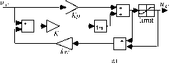 limitl -ч>ви limit2 imit3 FIGURE 19.16 (a) pi implementation with antiwindup (usually l/Kp <k< KJKp) to deal with rectifier saturation; (b) pi with ramp limiter/soft starter {k Kp) and integral component limiter to deal with large perturbations. These approaches introduce zeros in the right half-plane (nonminimum phase systems), and/or extra poles, giving more realistic results. Taking a first-order approximation and root-locus techniques, it is found that the rectifier is stable for Tp > KpkT/ipRt) (C > 0.25). Another approach uses the conditions of magnitude and angle of the delay function Q-sT/2p obtain the system root locus. Also, the power converter can be considered a sampled data system, at frequency p/T, and Z transform can be used to determine the critical gain and first frequency of instability p/(2T), usually half the switching frequency of the rectifier. Example 19.7. Buck-Boost dc/dc Converter Feedback Design in the Discontinuous Mode. The methodologies just described do not apply to power converters operating in the discontinuous mode. Fiowever, the derived equivalent averaged circuit approach can be used, calculating the mean value of the discontinuous current supplied to the load, to obtain the equivalent circuit. Consider the buck-boost converter of Example 19.1 (Fig. 19.1) with the new values Ц = 40 iH, Q = 1000 iF, = 15 Q. The mean value of the current i (Fig. 19.17b), supplied to the output capacitor and resistor of the circuit operating in the discontinuous mode, can be calculated noting that, if the input Vjq and output voltages are essentially constant (low ripple), the inductor current rises hnearly from zero, peaking at Ip = (Vp/A)! (Щ- 19.17a). As the mean value of ii, supposed hnear, is I = (Ipd2T)/2T), using the steady state input-output 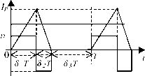  a) b) FIGURE 19.17 (a) Waveforms of the buck-boost converter in the discontinuous mode; (b) equivalent averaged circuit. relation Vci = 02 the above Ip value, 4 can be written: denominator of (19.52), usually С V2/2 and (On < InfJlO. Therefore: 21; к (19.50) Tp = KcvK/icolC,) T, = Tp(2i:cOnC,R, - l)/(KcvkM (19.53) This is a nonhnear relation that could be hnearized around an operating point. However, power converters in the discontinuous mode seldom operate just around an operating point. Therefore, using a quadratic modulator (Fig. 19.18), obtained integrating the ramp r(t) (Fig. 19.6a) and comparing the quadratic curve to the term upiVg/VQ (which is easily implemented using the Unitrode UC3854 integrated circuit), the duty cycle is Si = y/upiVo/iumaxDc) coustaut incremental factor Kqy can be obtained: cv - 2щ max-i (19.51) Considering zero voltage perturbations, the equivalent averaged circuit (Fig. 19.17b) can be used to derive the output voltage to input current transfer function v,(s)/iLo(s) = Ro/(sC,R,l). Using a PI controller (19.37), the closed-loop transfer function is: Vo(s) oref(s) Kcv(l+sT,)/CJp s2 + s(Tp + T,KcvkM/C,RJp + KcvK/CJp (19.52) Since two degrees of freedom exist, the PI constants are derived imposing С and ш„ for the second-order The transient behavior of this converter, with С = 1 and ш„я/10, is shown in Fig. 19.20a. Compared to Example 19.2, the operation in the discontinuous conduction mode reduces, by one, the order of the state-space averaged model and eliminates the zero in the right half of the complex plane. The inductor current does not behave as a true state variable, since during the interval ST this current is zero, and this value is always the current initial condition. Given the differences between these two examples, care should be taken to avoid the operation in the continuous mode of converters designed and compensated for the discontinuous mode. This can happen during turn-on or step load changes and, if not prevented, the feedback design should guarantee stability in both modes (Example 19.8, Fig. 19.20a). Example 19.8. Feedback Design for the Buck-Boost dc/dc Converter Operating in the Discontinuous Mode and Using Current Mode Control. The performances of the buck-boost converter operating in the discontinuous mode can be greatly enhanced if a current mode control scheme is used, instead of the voltage mode controller designed in Eample 19.7. Current mode control in power converters is the simplest form of state feedback. Current mode needs the measurement of the current ii (Fig. 19.1) but greatly simplifies the modulator design (compare Fig. 19.18 to 19.19), since no modulator linearization is used. The measured value, proportional to the current ii, is compared to the value upj given by the output voltage controller (Fig. 19.19). The modulator switches off the power semiconductor when kjlp = upj. Reset f 1- lock Quadratic modulator FIGURE 19.18 Block diagram of a pi controlled (feed-forward linearized) buck-boost converter operating in the discontinuous mode. oref Reset clock Modulator dj(s) Switching cell andL. Ч K- sCR+\ FIGURE 19.19 Block diagram of a current mode controlled buck-boost converter operating in the discontinuous mode. Expressed as a function of the peak current Ip, IiQ becomes (see the previous example) 4 = piDc/(2o) considering the modulator task ho - cP/iDc/(27o)- small perturbations, the incremental gain is Кем = oIcpi = УвсИМ' An 4 current delay = 1/(2/), related to the switching frequency can be assumed. The current mode control transfer function GmC) is: CM is) 1 + sTrf -- (19.54) Using the approach of Example 19.6, the values for and Tp are given by (19.55). Тр = 41:КсмККЛ (19.55) The transient behavior of this converter, with С = 1 and maximum value for Ip, /pax = 1 is shown in Fig. 19.20b. The output voltage step response presents no overshoot, no steady-state error, and better dynamics, compared to the response (Fig. 19.20a) obtained using the quadratic modulator (Fig. 19.18). Notice that, with current mode control, the converter behaves like a reduced-order system and the right half-plane zero is not present. The current mode control scheme can be advantageously applied to converters operating in the continuous mode, guarantying short-circuit protection, system order reduction, and better performances. Fiowever, for converters operating in the step-up (boost) regime, a stabilizing ramp with negative slope is required, to ensure stability (the stabilizing ramp will transform the signal Щр1 in a new signal upj - Yem(kt/T) where k is the needed amplitude for the compensation ramp and the function rem is the remainder of the division of kt by T. In the next section, current control of power converters will be detailed. Closed-loop control of resonant converters can be achieved using the outlined approaches, if the resonant
 0.02 0.02 920 110 §60 120 i. 0.005 sr 0 0.005 0.01 t[s] 0.01 tlsl 0.015 0.02 0.015 0.02 FIGURE 19.20 Transient response of the compensated buck-boost converter in the discontinuous mode. At = 0.001 s vjj- step from 23 V to 26 V. At = 0.011 s Vqjj- step from 26 V to 23 V. Top graphs: square reference vjj- and output voltage v. Bottom graphs: pulses, current; trace peaking at 40, 10 X (vjj- - Vq). (a) PI controlled and feed-forward linearized buck-boost converter with С = 1 and ~ nfj 10; (b) current mode controlled buck-boost with с = 1 and maximum value Д^ = 15 A. 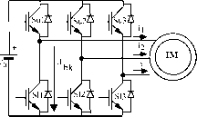 the rectangular waveform, which describes the inverter к leg state: FIGURE 19.21 igbt based voltage-sourced three-phase inverter with induction motor. phases of operation last for smaU intervals compared to the fundamental period. Otherwise, the equivalent averaged circuit concept can often be used and linearized, now considering the resonant converter input-output relations, normally functions of the driving frequency and input or output voltages, to replace the 3i variable. Example 19.9. Output Voltage Control in Three-Phase Voltage-Source Inverters using Sinusoidal Wave FWM (SWPWM) and Space Vector Modulation (SVM) Sinusoidal Wave PWM Voltage-source three-phase inverters (Fig. 19.21) are often used to drive squirrel-cage induction motors (IMs) in variable speed applications. Considering almost ideal power semiconductors, the output voltage щ^(к e {1, 2, 3}) dynamics of the inverter is negligible as the output voltage can hardly be considered a state variable in the time scale describing the motor behavior. Therefore, the best-known method to create sinusoidal output voltages uses an open-loop modulator with low-frequency sinusoidal waveforms sin(a;t), with amplitude defined by the modulation index (m G [0, 1]), modulating high-frequency triangular waveforms r(t) (carriers). Fig. 19.22, a process similar to the described in (19.4). This sinusoidal wave PWM (SWPWM) modulator generates the variable y, represented in Fig. 19.22 by 1 when sin(a;t) > r(t) 0 when sin(a;t) < r(t) (19.56) The turn-on and turn-off signals for the к leg inverter switches are related with the variable as follows: 1 then SUjt is on and Sl is off 0 then SUjt is off and Sl is on (19.57) This applies constant-frequency sinusoidally weighted PWM signals to the gates of each insulated gate bipolar transistor (IGBT). The PWM signals for all the upper IGBTs (Зщ, к G {1, 2, 3}) must be 120° out of phase and the PWM signal for the lower IGBT Sl must be the complement of the Su signal. Since transistor turn-on times are usually shorter than turn-off times, some dead time must be included between the Su and Sl pulses to prevent internal short circuits. Sinusoidal PWM can be easily implemented using a microprocessor or two digital counters/timers generating the addresses for two lookup tables (one for the triangular function, another for supplying the per unit basis of the sine, whose frequency can vary). Tables can be stored in read only memories, ROM, or erasable programmable ROM, EPROM. One multiplier for the modulation index (perhaps into the digital-to-analog (D/A) converter for the sine ROM output) and one hysterisis comparator must also be included. With SWPWM the first harmonic maximum amplitude of the obtained hne to line voltage is only about 86% of the inverter dc supply voltage V. Since it is expectable that this amplitude should be closer to V, different modulating voltages (for example, adding a third-order harmonic with 1/4 of the fundamental sine amplitude) can be used as long as the fundamental harmonic of the line to line voltage is kept sinusoidal. Another way is to leave SWPWM and consider the eight Constant Modulation Index ndexi> Produc Sine Wave к (PU) Repeating Sequence r(t) PU gamak Sum Relay Hysterisis 10-5 High outut=1 Low output=0 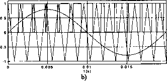 0.02 FIGURE 19.22 (a) swpwm modulator schematic; (b) main swpwm signals. .sector 0  FIGURE 19.23 a-p space vector representation of the three-phase bridge inverter leg base vectors. possible inverter output voltages trying to directly use then. This will lead to space vector modulation. Space Vector Modulation Space vector modulation (SVM) is based on the polar representation (Fig. 19.23) of the eight possible base output voltages of the three-phase inverter (Table 19.1, where v, Vf are the vector components of vector У^, g g {0, 1, 2, 3, 4, 5, 6, 7}, obtained with (19.58)). Therefore, as all the available voltages can be used, SVM does not present the voltage limitation of SWPWM. Furthermore, being a vector technique, SVM fits nicely with vector control methods often used in IM drives. Va (19.58) Consider that the vector (magnitude V, angle Ф) must be apphed to the IM. Since there is no such vector available directly, SVM uses an averaging technique to apply the two vectors, and closest to V. The vector Vl will be applied during SjT, while vector V2 will last SqT (where l/T is the inverter switching frequency, dj and 3 are duty cycles, 3 g [0, 1]). TABLE 19.1 The three-phase inverter 8 possible combinations, vector numbers, and respective components
 ij i ! vr FIGURE 19.24 Symmetrical SVM. If there is any leftover time in the PWM period T, then the zero vector is applied during time 3qT = - 3jT - З^Т^. Since there are two zero vectors (Vq and V7) a symmetric PWM can be devised, which uses both Vq and V7, as shown in Fig. 19.24. Such a PWM arrangement minimizes the power semiconductor switching frequency and IM torque ripples. The input to the SVM algorithm is the space vector V5, into the sector 5 , with magnitude and angle Ф^. This vector can be rotated to fit into sector 0 (Fig. 19.23) reducing to the first sector, Ф = Ф^ - 5 я/3. For any that is not exactly along one of the six nonnuU inverter base vectors (Fig. 19.23), SVM must generate an approximation by applying the two adjacent vectors during an appropriate amount of time. The algorithm can be devised considering that the projections of onto the two closest base vectors are values proportional to 3j and 3 duty cycles. Using simple trigonometric relations in sector 0 (0 < Ф < я/3) of Fig. 19.23, and considering Kj the proportional ratio, 3j and 3 are, respectively, 3j = KjOA and 3 = KjOB, yielding: sing-ф) (19.59) The Kj value can be found if we notice that when \> = \>j, = 1 and = 0 (or when \> = 5 = 0 and = 1). Therefore, since when = V, Vs = /vl + vl = V273Ф = 0, or when V, = У2. V, = 7273 V Ф = n/3, Kj = V3/(V2yj. Hence: the Kr constant IS V2K . /7t (19.60) The obtained resuhing vector cannot extend beyond the hexagon of Fig. 19.23. This can be understood if the maximum magnitude V of a vector with Ф = n/6 is calculated. Since, for Ф = я/6, = 1/2 and = 1/2 are the maximum duty cycles, from (19.60) sm = a/V2 is obtained. This magnitude is lower than that of vector since the ratio between these magnitudes is а/З/2. To generate sinusoidal voltages, the vector must be inside the inner circle of Fig. 19.23, so that it can be rotated without crossing the hexagon boundary. Vectors with tips between this circle and the hexagon are reachable, but produce nonsinusoidal line-to-line voltages. For sector 0 (Fig. 19.23), SVM symmetric PWM switching variables (y, 7з) and intervals (Fig. 19.24) can be obtained by comparing a triangular wave with amplitude и^тх (Fig- 19-24 where r(t) = 2uj/T, t g [0, T,/2]) with the following values: Qcmax с cmax /-t с с \ CI cmax A - -:r~ -(l + S-Ss) (19.61) Сметах fO I с i 5: \ cmax /1,5: 1 5: \ Therefore, y, у2, 7з are: 7i = 72 =
(19.64) Supposing that the space vector is now specified in the orthogonal coordinates (v, i5), instead of magnitude and angle Ф^, the duty cycles can be easily calculated knowing that = cos Ф, i; = sen Ф and using (19.60): (19.65) This equation enables the use of (19.63) and (19.64) to obtain SVM in orthogonal co-ordinates. Using SVM or SWPWM, the closed-loop control of the inverter output currents (induction motor stator currents) can be performed using an approach similar to that outlined in Example 19.6 and decouphng the currents expressed in a dq rotating frame. Extension of Eq. (19.61) to aU six sectors can be done if the sector number 5 is considered, together with the auxiliary matrix S: -1-111 1-1 -1 111-1-1 (19.62) Generalization of values Q, Q, and Q, denoted Q, Q, and Q, are written in (19.63), knowing that, for example, S((5+4)jnoj is the S matrix row with number 1 + (5 + 4)mod 6. ((5 Lod 6+1) Asn - И + 1 ((5 +4Ud 6+1) 6+1)  (19.63) 19.3 Sliding Mode Control of Power Converters 19.3.1 Introduction All the designed controUers for power converters are in fact variable structure controllers, in the sense that the control action changes rapidly from one to another of, usually, two possible S values, cyclically changing the converter topology. This is accomphshed by the modulator (Fig. 19.6), which creates the switching function S(t) imposing S(t) = 1 or S(t) = 0, to turn on or off the power semiconductors. As a consequence of this discontinuous control action, indispensable for efficiency reasons, state trajectories move back and forth around a certain average surface in the state space, and variables present some ripple. To avoid the effects of this ripple in the modehng and to apply linear control methodologies to time variant systems, average values of state variables and state space averaged models or circuits were presented (Section 19.2). However, a nonlinear approach to the modeling and control problem, taking advantage of the inherent ripple and variable structure behavior of power converters, instead of just trying to live with them, would be desirable, especially if enhanced performances could be attained. In this approach power converter topologies, as discrete nonlinear time-variant systems, are controUed to switch from one dynamics to another when just needed. If this switching occurs at a very high frequency (theoretically infinite), the state dynamics, described as (19.2) or (19.3), can be enforced to slide along a certain prescribed state space trajectory. The converter is said to be in sliding mode, the allowed deviations from the trajectory (the ripple) imposing the practical switching frequency. Sliding-mode control of variable structure systems, such as power converters, is particular interesting because of the inherent robustness, capability of system order reduction, and appropriateness to the on-off switching of power semiconductors [15,16]. The control action, being the control equivalent of the management paradigm just in time (JIT), provides timely and precise control actions, determined by the control law and the allowed ripple. Therefore, the switching frequency is not constant over all operating regions of the converter. This section treats the derivation of the control (sliding surface) and switching laws, robustness, stabihty, constant-frequency operation, and steady-state error elimination necessary for sliding-mode control of power converters, also giving some examples. 19.3.2 Principles of Sliding-Mode Control Consider the state-space switched model (19.3) of a power converter subsystem, and input-output linearization or another technique, to obtain, from state-space equations, one equation (19.66), for each controllable subsystem output у = X. In the controllability canonical form [11] (also known as input-output decoupled or companion form), (19.66) is: - [Xj,...,Xj i,Xjf = [xj,i, ..., Xj, -Л(х) - pM + h(x)uj,(t)f (19.66) where x = [xj, ..., Xj i, Xjf is the subsystem state vector, fi(x) and b/j(x) are functions of x, p/j(t) represents the external disturbances, and (t) is the control input. In this special form of state-space modeling, the state variables are chosen so that the x variable (i G {/г, ..., j - 1}) is the time derivative of that is X = [xj, Xj, Xj, ..., x, where m = j - h [9]. 19.3.2.1 Control law (Sliding Surface) The required closed-loop dynamics for the subsystem output vector у = X can be chosen to verify (19.67) with selected values. This is a model reference adaptive control approach to impose a state trajectory that advantageously reduces the system order j - h-\- 1. t=h j (19.67) Effectively, in a single-input/single-output (SISO) subsystem the order is reduced by one unity, applying the restriction (19.67). In a multiple-input/multiple-output (MIMO) system. in which V independent restrictions could be imposed (usually with V degrees of freedom), the order could often be reduced in V units. Indeed, from (19.67), the dynamics of the jth term of X is linearly dependent from the j - h first terms: dt hkj hkjdt (19.68) The controllability canonical model allows the direct calculation of the needed control input to achieve the desired dynamics (19.67). In fact, as the control action should enforce the state vector x, to follow the reference vector x = [xj, ic/j , 3c;j , ..., Xj ], the tracking error vector will be e = К - /z j-lr - i-l Ч = [x, xj-V ejf. Thus, if we equate the subexpressions for dxj/dt of (19.66) and (19.67), the necessary control input Uj(t) is: P/z(0+A(x) + (19.69) р,(0+л(х)-Ет.+1, + Ет i=h / i=h b,(x) This expression is the required closed-loop control law, but unfortunately it depends on system parameters and external perturbations and is difficult to compute. Moreover, for some output requirements, Eq. (19.69) would give extremely high values for the control input W/j(t), which would be impractical or almost impossible. In most power converters Ui(t) is discontinuous. Yet, if we assume one or more discontinuity borders dividing the state space into subspaces, the existence and uniqueness of the solution is guaranteed out of the discontinuity borders, since in each subspace the input is continuous. The discontinuity borders are subspace switching hypersurfaces, whose order is the space order minus one, along which the subsystem state slides, since its intersections of the auxiliary equations defining the discontinuity surfaces can give the needed control input. Within the shding-mode control (SMC) theory, assuming a certain dynamic error tending to zero, one auxiliary equation (sliding surface) and the equivalent control input (t) can be obtained, integrating both sides of (19.68) with null initial conditions: (19.70) This equation represents the discontinuity surface (hyper-plane) and just defines the necessary sliding surface S(x, t) to obtain the prescribed dynamics of (19.67): S(x 0 = E к,г = 0 (19.71) In fact, by taking the first time derivative of S(x, t), t) = 0, solving it for dxj/dt, and substituting the result in (19.69), the dynamics specified by (19.67) is obtained. This means that the control problem is reduced to a first-order problem, since it is only necessary to calculate the time derivative of (19.71) to obtain the dynamics (19.67) and the needed control input W/j(t). ад = (5 + шХ = m = 0 Bj(s) = 1 m = 1 Bj(s) = 5 + m = 2 = Bj(s) = 5 + 2ш^5 + col m = 3 Bj(s) - 5 + 3co,s + 3605 + col m = 4 Bj(s) = 5 + 4ш,5 + 6cdI + 46025 + 4ш^5 + (19.72a) hAE(s)m - m = 0 = m = 2 TA£() m = 3 TA£() m = 4 Itje(s) Itae(s) = 1 5 + 1.4Ш^5 + Ш^ 5 + 1.75ш,52+2.15ш25 + ш^, (19.72b) m = 0 Be(s) m = 1 5(5) = 5t, + 1 m = 2 = m = 3 = ((5t,) + 3.6785t, + 6.459)(5t, + 2.322) 15 (st,f + 6(st,f + 155t, + 15 15 m = 4 5(5) = (st,f + 10(5 + 45(5 + 105(5 + 105 105 (19.72c) The shding surface (19.71), as the dynamics of the converter subsystem, must be a Routh-Hurwitz polynomial and verif) the shding manifold invariance conditions, S(Xp t) = 0 and S(xi, t) = 0. Consequently, the closed-loop controUed system behaves as a stable system of order j - h whose dynamics is imposed by the coefficients k, which can be chosen by pole placement of the poles of the order m = j - h polynomial. Alternatively, certain kinds of polynomials can be advantageously used (19.77): Butterworth, Bessel, Chebyshev, eUiptic (or Cauer), binomial, and minimum integral of time absolute error product (ITAE). Most useful are Bessel polynomials Be(s), which minimize the system response time t, providing no overshoot, the polynomials Itae(s) that minimize the ITAE criterion for a system with desired natural oscillating frequency ш^, and binomial polynomials Bj(s). For m > 1, ITAE polynomials give faster responses than binomial polynomials. These polynomials can be the reference model for this model reference adaptive control method. 19.3.2.2 Closed-Loop Control Input-Output Decoupled Form For closed-loop control applications, instead of the state variables x, it is worthy to consider, as new state variables, the errors e components of the error vector e = [e, e, ё^,..., eJ of the state-space variables x, relative to a given reference x (19.74). The new controUability canonical model of the system is: = [e,-fXe) + pXt) - bXe)uMf (19.73) where/g(e), pe(t), and Ь^(е) are functions of the error vector e. As the transformation of variables e, = X: - X: with i = h, ... ,j (19.74) is linear, the Routh-Hurwitz polynomial for the new sliding surface S(e t) is (19.75) Since e.(s) = se,(s), this control law, that from (19.72) can be written S(e, 5) = e,(s + co), does not depend on circuit parameters, disturbances or operating conditions, but only on the imposed k parameters and on the state variable errors e which can usually be measured or estimated. The control law (19.75) enables the desired dynamics of the output variable(s), if the semiconductor switching strategy is designed to guarantee the system stabUity. In practice, the finite switching frequency of the semiconductors wiU impose a certain dynamic error г tending to zero. The control law (19.75) is the required controUer for the closed loop SISO subsystem with output y. 1 ... 42 43 44 45 46 47 48 ... 91 |
|
© 2026 AutoElektrix.ru
Частичное копирование материалов разрешено при условии активной ссылки |