 |
 |
 |
| Главная Журналы Популярное Audi - почему их так назвали? Как появилась марка Bmw? Откуда появился Lexus? Достижения и устремления Mercedes-Benz Первые модели Chevrolet Электромобиль Nissan Leaf |
Главная » Журналы » Metal oxide semiconductor 1 ... 43 44 45 46 47 48 49 ... 91 19.3.2.3 Stability 193,23,1 Existence Condition The existence of the operation in shding mode imphes S(e., t) = 0. Also, to stay in this regime, the control system should guarantee S{e t) = 0. Therefore, the semiconductor switching law must ensure the stability condition for the system in sliding mode, written as S(e., t)S{e t) <0 (19.76) The fulfillment of this inequality ensures the convergence of the system state trajectories to the sliding surface S(e., t) = 0, since If 5(,0 >0 and 5(,0 <0, then 5(,0 will decrease to zero . If S(e.,t)<0 and S(e.,t)>0, then S(e., t) will increase toward zero Hence, if (19.76) is verified, then S(e t) will converge to zero. The condition (19.76) is the manifold S(e t) invariance condition, or the shding mode existence condition. Given the state-space model (19.73), the function of the error vector e, and, from S(e t) = 0, the equivalent average control input Uq(t) that must be applied to the system in order that the system state slides along the surface (19.75), is given by[5] de de, de - Щё) (19.77) This control input Uq(t) ensures converter subsystem operation in the shding mode. 19,3,2,3,2 Reaching Condition The fulfillment of S(e., t)S(e., t) < 0, as S(e., t)S(e., t) = (l/2)S(e t) imphes that the distance between the system state and the shding surface will tend to zero, since S(e t) can be considered a measure for this distance. This means that the system will reach sliding mode. Additionally, from (19.73) it can be written d dt =-fe(e)+pXt)-bXe)uM (19.78) From (19.75), Eq. (19.79) is obtained. S(e..t) = j:k,e, dm e. (19.79) If S(e., t) > 0, from the Routh-Fiurwitz property of (19.75), then e, > 0. In this case, to reach S(e t) = 0 it is necessary to impose -bXe)ui(t) = - U in (19.78), with U chosen to guarantee dedt < 0. After a certain time, e, will be = deJdt < 0, implying along with (19.79) that s(e t) < 0, thus verifying (19.76). Therefore, every term of S(e t) will be negative, which implies, after a certain time, an error e < 0 and S(e t) < 0. Fience, the system will reach sliding mode, staying there if (7 = Uq(t). This same reasoning can be made for S(e t) < 0, it now being necessary to impose - b(e)ui(t) = +(7, with U high enough to guarantee dejdt > 0. To ensure that the system always reaches sliding-mode operation, it is necessary to calculate the maximum value of Uq(t), Uqmax and also imposc the reaching condition: и > U,q (19.80) This means that the power supply voltage values U should be chosen high enough to additionally account for the maximum effects of the perturbations. With step inputs, even with и > Uq, the converter usually loses sliding mode, but it will reach it again, even if the Uq is calculated considering only the maximum steady-state values for the perturbations. 19.3.2.4 Switching Law From the foregoing considerations, supposing a system with two possible structures, the semiconductor switching strategy must ensure S(e t)S(e t) < 0. Therefore, if S(e t) > 0, then S (e t) < 0, which imphes, as seen, -b(e)ui(t) = - U (the sign of bg(e) must be known). Also, if S(e t) < 0, then S(e t) > 0, which implies -b(e)ui(t) = -\-U. This imposes the switching between two structures at infinite frequency. Since power semiconductors can switch only at finite frequency, in practice, a small enough error for S(e., t) must be allowed (-г < S(e, t) < +e). Fience, the switching law between the two possible system structures must be U/bXe)for S(e,t) > +e -U/bXe) for S(e., t) < -в (19.81) The condition (19.81) determines the control input to be applied and therefore represents the semiconductor switching strategy or switching function. This law determines a two-level pulse width modulator with just in time switching (variable frequency). 19.3.2.5 Robustness The dynamics of a system with closed-loop control using the control law (19.75) and the switching law (19.81), does not depend on the system operating point, load, circuit parameters, power supply, or bounded disturbances, as long as the control input Ui(t) is large enough to maintain the converter subsystem in sliding mode. Therefore, it is said that the power converter dynamics, operating in sliding mode, is robust against changing operating conditions, variations of circuit parameters, and external disturbances. The desired dynamics for the output variable(s) is determined only by the coefficients of the control law (19.75), as long as the switching law (19.81) maintains the converter in sliding mode. 19.3.3 Constant-Frequency Operation Prefixed switching frequency can be achieved, even with sliding-mode controUers, at the cost of losing the JIT action. As the sliding-mode controUer changes the control input when needed, and not at a certain prefixed rhythm, applications needing constant switching frequency (such as thyristor rectifiers or resonant converters) must compare S(e t) (hysteresis width 2i much narrower than 2e) with auxUiary triangular waveforms (Fig. 19.25a), auxiliary sawtooth functions (Fig. 19.25c), three-level clocks (Fig. 19.25d), or phase-locked loop control of the comparator hysterisis variable width 2e. However, as illustrated in Fig. 19.25b, steady-state errors do appear. Often, they should be eliminated as described in the next section. 19.3.4 Steady-state Error Elimination in Converters with Continuous Control Inputs In the ideal sliding mode, state trajectories are directed toward the sliding surface (19.75) and move exactly along the discontinuity surface, switching between the possible system structures, at infinite frequency. Practical shding modes cannot switch at infinite frequency, and therefore exhibit phase plane trajectory osciUations inside a hysterisis band of width 2e, centered in the discontinuity surface. The switching law (19.75) permits no steady-state errors as long as S(e t) tends to zero, which implies no restrictions on the commutation frequency. Control circuits operated at constant frequency, or needed continuous inputs, or particular limitations of the power semiconductors, such as minimum on or off times, can originate S(e t) = 8i ф 0. The steady-state error (eJ of the Xf variable, - = Sj/Zc/j, can be ehminated, increasing the system order by 1. The new state space controUabUity canonical form, considering the error e between the variables and their references, as the state vector, is d di dt, , ..., , = [e,, e ..., e. - /Де) - - K{t)u,{tf (19.82) The new sliding surface S{e t), written from (19.75) considering the new system (19.82), is e.,dt+j:ke.,0 (19.83) This sliding surface offers zero-state error, even if S(e t) = due to hardware errors or fixed (or limited) frequency switching. Indeed, in the steady state, the only nonnuU term is /cq \ xdt = Sj. Also, like (19.75), this closed-loop control law does not depend on system parameters or perturbations to ensure a prescribed closed-loop dynamics similar to (19.67) with an error approaching zero. The approach outlined herein precisely defines the control law (sliding surface (19.75) or (19.83)) needed to obtain the selected dynamics, and the switching law (19.81). As the control law aUows the implementation of the system controller, and the switching law gives the PWM modulator, there is no need to design linear or nonlinear controUers, based on hnear converter models, or devise off-line PWM modulators. Therefore, sliding-mode control theory, apphed to power converters, provides a systematic method to generate both the controUer(s) (usually nonlinear) and the modulator(s) that wiU ensure a model reference robust dynamics, solving the control problem of power converters. In the next examples, it is shown that shding-mode controllers use (nonhnear) state feedback, therefore needing to measure the state variables and often other variables, since they use more system information. This is a disadvantage since more sensors are needed. However, the straightforward control design and obtained performances are much better than those obtained with the averaged models, the use of more sensors uh(t) 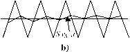 Sex,t Level Clock c) d) figure 19.25 Auxiliary functions and methods to obtain constant switching frequency with sliding-mode controllers. being really valued. Alternatively to the extra sensors, state observers can be used [9]. Example 19.10. Sliding-Mode Control of the Buck-Boost dc/dc Converter. Consider again the buck-boost converter of Fig. 19.1 and assume the converter output voltage to be the controlled output. From Section 19.2, using the switched state-space model (19.9), making dv/dt = 9, and calculating the first time derivative of 6, the controllability canonical model (19.84), where = v/R, is obtained: 1 - m (i-d(t)f -v - C,{\-b{t)) dt 1 di, (0(1 - bit)) C dt (19.84) This model, written in the form of (19.66), contains two state variables, and 9. Therefore, from (19.75) and considering = y - d , eg = 9,. - 9, the control law (sliding surface) is dt C (19.85) + io0 This sliding surface depends on the variable S(t), which should be precisely the result of the application, in (19.85), of a switching law similar to (19.81). Assuming an ideal up-down converter and slow variations, from (19.25b) the variable d{t) can be averaged to (5j = Vg/(v, + Vpc)- By substituting this relation in (19.85), and rearranging, (19.86) is derived: S(e ,0 = - - = о (19.86) This control law shows that the power supply voltage VjjQ must be measured, as well as the output voltage and the currents and ii. To obtain the switching law from stability considerations (19.76), the time derivative of S(e., t), supposing (Po + Vj)c)/Vq almost constant, is S(e .,t)=- CoK (0 + Уве /de, k.dv. 2 Or h di, ki dt2 Kc.dt (19.87) If S(e., 0 > 0 then, from (19.76), S(e., t) < 0 must hold. Analyzing (19.87), we can conclude that, if S(e t) > 0, S(e t) is negative if, and only if, dii/dt > 0. Therefore, for positive errors e > 0 the current il must be increased, which implies S(t) = 1. Similarly, for S(e., t) < 0, diJdt < 0 and 3(t) = 0. Thus, a switching law similar to (19.81) is obtained: 3(t) = 1 for S(e., t) > +£ 0 for S(e.,t) <-8 (19.88) The same switching law could be obtained from knowing the dynamic behavior of this nonminimum-phase up-down converter: to increase (decrease) the output voltage, a previous increase (decrease) of the ii current is mandatory. Equation (19.85) shows that, if the buck-boost converter is into sliding mode (S(e t) = 0), the dynamics of the output voltage error tends exponentially to zero with time constant /сз/с^. Since during step transients, the converter is in the reaching mode, the time constant /сз/с^ cannot be designed to originate error variations larger than allowed by the self-dynamics of the converter excited by a certain maximum permissible il current. Given the polynomials (19.72) with m = 1, ki/k2 = 0)g should be much lower than the finite switching frequency (1/ T) of the converter. Therefore, the time constant must obey /сз/с^ T. Then, knowing that and k are both imposed, the control designer can tailor the time constant as needed, provided that the preceding restrictions are observed. Short-circuit-proof operation for the sliding-mode controlled buck-boost converter can be derived from (19.86), noting that all the terms to the left of ii represent the set point for this current. Therefore, hmiting these terms (Fig. 19.26, saturation block, with max = 40 A), the switching law (19.88) ensures that the output current will not rise above the maximum imposed limit. Given the converter nonminimum-phase vorefj и Suml [T]- [jj>J k2/(kl*Co) Switching delta law 0.005 0.01 0.015 0.02 0.025 0.03 0.035 0.04 t[s]
0.005 0.01 0.015 0.02 0.025 0.03 0.035 0.04 tisl figure 19.26 (a) Block diagram of the sliding-mode nonlinear controller for the buck-boost converter; (b) transient responses of the sliding-mode controlled buck-boost converter. At = 0.005 s y step from 23 v to 26 v. At = 0.02 s Vj( step from 26 v to 23 v. Top graph: square reference y and output voltage v. Bottom graph: trace around 20, current; trace starting at zero, 10 x (vjr - v). behavior, this current limit is fundamental to reach the sliding-mode of operation with step disturbances. The block diagram (Fig. 19.26a) of the implemented control law ((19.86) with Q/ci c2 =4) and switching law ((19.88) with г = 0.3) does not included the time derivative of the reference (dvJdt) since, in a dc-dc converter its value is considered zero. The controller hardware (or software), derived using just the sliding-mode approach, operates only in closed loop. The resulting performance (Fig. 19.26b) is much better than that obtained with the PID notch filter (compare to Example 19.4, Fig. 19.9b), with a higher response speed and robustness against power-supply variations. Example 19.11. Sliding-Mode Control of the Single-Phase Half-Bridge Converter. Consider the half-bridge four quadrant converter of Fig. 19.27 with output filter and inductive load (Vj = 300 V; Увстгп = 230 V; = 0.1 Q; L, = 4 mH; C, = 470 цЕ; inductive load with nominal values R = 7 = 1 mH). 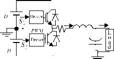 Assuming that power switches, output filter capacitor, and power supply are aU ideal, and a generic load with allowed slow variations, the switched state-space model of the converter, with state variables and ii, is
(19.89) where is the generic load current and ipwvf = (Odc is the extended PWM output voltage {d{t) = +1 when one of the upper main semiconductors of Fig. 19.27 is conducting and d{t) = -1 when one of the lower semiconductors is on). Output Current Control (Current Mode Control) To perform as a v voltage controUed ii current source (or sink) with transconductance (g = ii/ViJ, this converter must supply a current to the output inductor, obeying ii=gVi. Using a bounded v voltage to provide output short-circuit protection, the reference current for a shding-mode controUer must be % - SmiL- Therefore, the controUed output is the ii current and the controUability canonical model (19.90) is obtained from the second equation of (19.89), since the dynamics of this subsystem, being governed by S(t)Vj(j, is already in the controUabUity canonical form for this chosen output. figure 19.27 Half bridge power inverter with insulated gate bipolar transistors, output filter and load. di, R,. 1 , smc (19.90) iLr iLMax iL Switching law epsilon=+-2 Ы iLr iLMax iL
Suml error Comparatorb-O.Ol PWM triangle FIGURE 19.28 (a) Implementation of short-circuit-proof sliding-mode current controller (variable frequency); (b) implementation of fixed-frequency, short-circuit-proof, sliding-mode current controller using a triangular waveform. A suitable sliding surface (19.91) is obtained from (19.90), making e, = i - i. S(e,, t) = kpe = kp(ii - il) (19.91) The switching law (19.92) can be devised calculating the time derivative of (19.91) S(e-, t), and applying (19.76). If S(ei, t) > 0, then dJdt > 0 must hold to obtain S(ei, i) < 0, implying S(t) = 1. S(t) = 1 for S(e, t) > +£ - 1 for S(ei, t) < -8 (19.92) The kp value and allowed ripple 8 define the instantaneous value of the variable switching frequency. The sliding mode controller is represented in Fig. 19.28a. Step response (Fig. 19.29a) shows variable-frequency operation and a very short rise time (hmited only by the available power supply) and confirms the expected robustness against supply variations. For systems where fixed frequency operation is needed, a triangular wave, with frequency (10 kFiz) slightly greater than the maximum variable frequency, can be added (Fig. 19.28b) to the sliding-mode controller, as explained in Section 19.3.3. Performances (Fig. 19.29b), comparable to those of the variable-frequency sliding-mode controller show the constant switching frequency, but also a steady-state error dependent on the operating point. To eliminate this error, a new sliding surface (19.93), based on (19.83), should be used. The constants kp and /cq can be calculated, as discussed in Example 19.10. S(e,,t) = ko e.dt + kpe, = 0 (19.93) The new constant-frequency shding-mode current controller (Fig. 19.30a), with added antiwindup techniques (Example 19.6), since a saturation (errMax) is о I 40 t 0 i 0 i20L t ° --20 Variable switching frequency 0.005 0.01 0.015 0.02 0.005 0.01 0.015 0.02 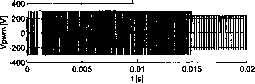  Constant switcNng frequency --20 0.005 0.01 0.015 0.02 JJsL 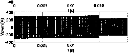 0.02 0.015 0.02 FIGURE 19.29 Performance of the transconductance amplifier; response to a step from -20 A to 20 A at Г = 0.001 s and to a Vj( step from 300 V to 230 V at r = 0.015 s. 1�9456 needed to keep the frequency constant, now presents no steady-state error (Fig. 19.30b). Performances are comparable to those of the variable frequency controUer, and no robustness loss is visible. The applied sliding-mode approach led to the derivation of the known average current-mode controller. Output voltage control To obtain a power operational amplifier suitable for buUding uninterruptible power supplies, power filters, power gyrators, inductance simulators, or power factor active compensators, must be the controUed converter output. Therefore, using the input-output linearization technique, it is seen that the first time derivative of the output (dv/dt) = (il - io)/C = в, does not explicitly contain the control input S(t)VDQ. Then, the second derivative must be calculated. Taking into account (19.89), as 0 = (il - i,)/C (19.94) is derived d4A, df dt dt\ Q R, . 1 di. l,C, L,C; Qdt d{t)Vi (19.94) This expression shows that the second derivative of the output depends on the control input d{t)VjjQ. No further time derivative is needed, and the state-space equations of the equivalent circuit, written in the phase canonical form, are d dt -Vn-- T С T с i + (19.95) According to (19.75), (19.95), and (19.89), considering that e is the feedback error e = v, - v a sliding surface S(e , t), can be chosen: S(e t) = kie.k2 , к2е de = y(4-o) + Q + i,-i, = o (19.96) where is the time constant of the desired first-order response of output voltage ( > T > 0), as the strong relative degree [9] of this system is 2, and sliding-mode operation reduces by one the order of this system (the strong relative degree represents the number of times the Sum2 Ш Limited Integ-ator еп-Мах FWM triansfe CoinparatoiH-0.02 > 40 =K-20 40 5-20  0.005 0.01 0.015 0.02 --20 dclU 0  0.005 0.01 0.015 0.02 400 200 I 0 >-200 400 0 0.005 0.01 0.015 0.02 tls] figure 19.30 (a) Block diagram of the average current-mode controller (sliding mode); (b) performance of the fixed-frequency sliding-mode controller with removed steady-state error: response to an step from -20 A to 20 A at = 0.001 s and to a F- step from 300 V to 230 V at = 0.015 s. output variable must be time differentiated until a control input explicitly appears). Calculating S(e, t), the control strategy (switching law) (19.97) can be devised since, if S(e, t) > 0, diJdt must be positive to obtain S(e, t) < 0, implying S(t) = 1. Otherwise, S(t) = -1. MA-I lforS(.,,t)>0(t;pM = +Dc) - \ -1 for S(e,, t) < 0 (vpm = -Vdc) In the ideal sliding-mode dynamics, the filter input voltage Vpym switches between Vq and - Vc ih infinite frequency. This switching generates the equivalent control voltage V that must satisfy the sliding manifold invariance conditions, S{e, t) = 0 and S{e, t) = 0. Therefore, from S{e, t) = 0, using (19.96) and (19.89), (or from (19.94)),V, is: V~df P dt PL,C, PC, Q dt J (19.98) This equation shows that only smooth input v, signals ( smooth functions) can be accurately reproduced at the inverter output, as it contains derivatives of the signal. This fact is a consequence of the stored electromagnetic energy. The existence of the sliding-mode operation implies the following necessary and sufficient condition: -Vdc < Ущ < Уве (19.99) Equation (19.99) enables the determination of the minimum input voltage V needed to enforce the sliding-mode operation. Nevertheless, even in the case of \Vq\ > \ Vp)cl the system experiences only a saturation transient and eventually reaches the region of sliding-mode operation, except if, in the steady state, operating point and disturbances enforce V > Vq \. In the ideal shding mode, at infinite switching frequency, state trajectories are directed toward the sliding surface and move exactly along the discontinuity surface. Practical power converters cannot switch at infinite frequency, so a typical implementation of (19.96) (Fig. 19.31a) with neglected v,) features a comparator with hysterisis 2e, switching occurring at \S(e, t)\ > 8 with frequency depending on the slopes of il. This hysterisis causes phase plane trajectory oscillations of width 28 around the discontinuity surface S(e, t) = 0, but the V voltage is still correctly generated, since the resulting duty cycle is a continuous variable (except for error limitations in the hardware or software, which can be corrected using the approach pointed out by (19.82)). The design of the compensator and modulator is integrated with the same theoretical approach, since the signal S(e , t) applied to a comparator generates the pulses for the power semiconductors drives. If short-circuit-proof operation is built into the power semiconductor drives, there is the possibility to measure only the capacitor current (ii - iJ. Short-Circuit Protection and Fixed Frequency Operation of the Power Operational Amplifier If we note that all the terms to the left of ii in (19.96) represent the value of ii , a simple way to provide short-circuit protection is to bound the sum of all these terms (Fig. 19.31a) with i = 100 A). Alternatively, the output current controllers of Fig. 19.28 can be used, comparing (19.91) to (19.96), to obtain i = S(e, , t)/ kp-\-ii. Therefore, the block diagram of Fig. 19.31a provides the ii output (for kp = 1) to he the input of the current controllers (Figs. 19.28 and 19.31a). As seen, the controllers of Figs. 19.28b and 19.30a also ensure fixed-frequency operation. For comparison purposes a proportional integral (PI) controller, with antiwindup (Fig. 19.31b) for output voltage control, was designed, supposing current mode control of the half bridge (modeled considering a small delay T, i = gViJ(l + sT), a pure resistive load R evo Co*kl/k2 + Sana iLrMa jSwitohing delta 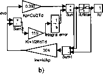 FIGURE 19.31 (a) Implementation of short-circuit-proof, sliding-mode output voltage controller (variable frequency); (b) implementation of antiwindup PI current mode (fixed-frequency) controller. Sliding mode
 0.02 0.02 Sliding mode (Ro*20) 200 100 л-100 S.200 0.005 0.01 t[s] 0.015 0.02 100 50 ? -50 0
0.005 0.01 t[s] 0.015 0.02 a) Variable firequency sliding mode (nominal load) b) Variable frequency sliding mode {Ro>20) FIGURE 19.32 Performance of the power operational amplifier; response to a v step from -200 V to 200 V at t = 0.001 s and to a Vc step from 300 V to 230 V at = 0.015 s. and using the approach outlined in Examples 19.6 and 19.8 (k, = 1, g = 1, = 0.5, = 600 is)). The obtained PI (19.37) parameters are = RoCo (19.100) Both variable-frequency (Fig. 19.32) and constant frequency (Fig. 19.33) shding-mode output voltage controllers present excellent performance and robustness with nominal loads. With loads much higher than the nominal value (Figs. 19.32b and Fig. 19.33b), the performance and robustness are also excellent. The sliding-mode constant-frequency PWM controller presents the additional advantage of injecting lower ripple in the load. As expected, the PI regulator presents lower performance (Fig. 19.34). The response speed is lower and the insensitivity to power supply and load variations (Fig. 19.34b) is not as high as with sliding mode. Nevertheless, the PI performances are acceptable, since its design was carried considering a slow and fast manifold sliding mode approach: the fixed-frequency shding-mode current controller (19.93) for the fast manifold (the il current dynamics) and the antiwindup PI for the slow manifold (the voltage dynamics, usually much slower than the current dynamics). Example 19.12. Constant-Frequency Sliding-Mode Control of p Pulse Parallel Rectifiers. This example presents a new paradigm to the control of thyristor rectifiers. Since p pulse rectifiers are variable-structure systems, shding-mode control is applied here to 12 pulse rectifiers, still useful for very high power apphcations [12]. The design determines the variables to be measured and the controlled rectifier presents robustness and much shorter response times, even with parameter uncertainty, perturbations, noise, and nonmodeled dynamics. These Fixed frequency sliding mode § 200 f -100 f-200 0.005 0.01 tls] 0.015 0.02 -100 I 50 > г -50 0
0.005 0.01 t[s] 0.015 0.02 Fixed frequency sliding nrode (Ro20) 200 100 4-100 2-200 0 0.005 0.01 0.015 0.02 0 0.005 0.01 tls] 0.015 0.02 a) Fixed frequency sliding mode (nominal load) b) Fixed frequency sliding mode (Л^х^О) FIGURE 19.33 Performance of the power operational amplifier; response to a i; step from -200 V to 200 V at t = 0.001 s and to a Vc step from 300 V to 230 V at = 0.015 s. ��:.72:/.+6+A 19 Control Methods for Power Converters PI & current mode
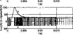
1-100 I 50 - 0 0.005 0.01 t[sl 0.015 0.02 0.005 0.015 0.02 PI& current mode (Ro*20) ! 200 100 w-lOO 1-200 0.005 0.015 0.02 0 0.005 0.01 0.015 0.02 0 0.005 0.01 0.015 0.02 t[s] 2 Л figure 19.34 Performance of the PI controlled power operational amplifier; response to a г; step from -200 V to 200 Vat t = 0.001 s and to a Vj) step from 300V to 230Vat z = 0.015 s. performances are not feasible using linear controllers, obtained here for comparison purposes. Modeling the 12-Pulse Parallel Rectifier The 12-pulse rectifier (Fig. 19.35a) is buih with four three-phase half-wave rectifiers, connected in parallel with current-sharing inductances / and Г merged with capacitors C, c2, to obtain a second-order LC filter. This allows low output-voltage ripple and continuous mode of operation (laboratory model with / = 44 mFi; Г = 13 mFi; С = C2 = 10 mF; star-delta connected ac sources with Es 65 V and power rating 2.2 kW, load approximately resistive i 3 to 5 Q). To control the output voltage v, given the complexity of the whole system, the best approach is to derive a low-order model. By averaging the four half-wave rectifiers, neglecting the rectifier dynamics and mutual couphngs, the equivalent circuit of Fig. 19.35b is obtained (/ = /2 = /3 = /4 = /; k = k = Сц = Ci2 = C)- Since the rectifiers are identical, the equivalent 12-pulse rectifier model of Fig. 19.35c is derived, simplifying the resulting parallel associations (L = 1/4; L2 = r/2; Q = 2C). Considering the load current as an external perturbation and Vl the control input, the state-space model of the equivalent circuit Fig. 19.3.5c is: 1/Q -1/Q 0 I/c2 1/Li 0 0 -1/Qj -l/Ii -1/L2 (19.101) 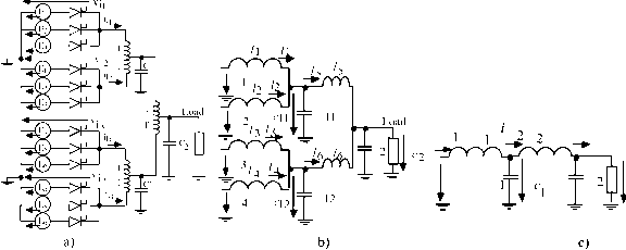 Load figure 19.35 Twelve-pulse rectifier with interphase reactors and intermediate capacitors; (b) rectifier model neglecting the half-wave rectifier dynamics; (c) low-order averaged equivalent circuit for the 12-pulse rectifier with the resulting output double LC filter. Sliding-Mode Control of the 12-Pulse Parallel Rectifier Since the output voltage v of the system must foUow the reference v, the system equations in the phase canonical (or controUability) form must be written, using the error e = v - v and its time derivatives as new state error variables, as done in Example 19.11. d di e - - C1L1C2 C1C2L2J dt C2 dt C1L1C2L2. (19.102) The shding surface S(e, t), designed to reduce the system order, is a linear combination of aU the phase canonical state variables. Considering (19.102), (19.101), and the errors e , Cq, ву, and e, the sliding surface can be expressed as a combination of the rectifier currents, voltages, and their time derivatives: S(e, t) = e, + keee + к^е^ + /с^е^ = v, + кев, + куу, + kpP, C2 dt2 Q C2L2 ka ka ka \C2 12 22/ = 0 (19.103) Equation (19.103) shows the variables to be measured (C2 % %) Therefore, it can be concluded that the output current of each three-phase half-wave rectifier must be measured. The existence of the sliding mode imphes S(e t) = 0 and 5(,0 = 0. Given the state models (19.101) (19.102), and from 5(,0 = 0, the available voltage of the power supply must exceed the equivalent average dc input voltage V (19.104), which should be applied at the filter input, in order that the system state slides along the sliding surface (19.103). v9ib(e, + key, + kA + kA) C2 L2 {в + к^,Р) + I c2l2 + + - QAQ2l7 + (k+L2)+CiLiL2 (19.104) This means that the power supply RMS voltage values should be chosen high enough to account for the maximum effects of the perturbations. This is almost the same criterion adopted when calculating the RMS voltage values needed with linear controUers. However, as the voltage contains the derivatives of the reference voltage, the system wiU not be able to stay in sliding mode with a step as the reference. The switching law would be derived, considering that, from (19.102), b,(e) > 0. Therefore, from (19.81), if S(e t) > +£, then Vi(t) = V, else if S(e t) < -г, then Vi(t) = - Veq - However, because of the lack of gate turn-off capabUity of the rectifier thyristors, power rectifiers cannot generate the high-frequency switching voltage Vi(t), since the statistical mean delay time is T/2p and reaches T/2 when switching from +Vg to - V. To control mains switched rectifiers, the described constant frequency sliding mode operation method is used, in which the sliding surface S(e t), instead of being compared to zero, is compared to an auxUiary constant frequency function r(t) (Fig. 19.6b) synchronized with the mains frequency. The new switching law is: И kpS(e, t) > r(t) i l{kpS(e,,t)<r(t)-i Trigger the next thyristor Do not trigger any thyristor Vi(t) (19.105) Since now S(e t) is not near zero, but around some value of r(t), a steady-state error appears (min[r(t)]/L < max[r(t)]/L), as seen in Exam- ple 19.11. Increasing the value of kp (toward the ideal saturation control) does not overcome this drawback, since oscillations would appear even for moderate kp gains, because of the rectifier dynamics. Instead, the sliding surface (19.106), based on (19.83), should be used. It contains an integral term, which, given the canonical controUabUity form and the Routh-Hurwitz property, is the only nonzero term in steady state. 1 ... 43 44 45 46 47 48 49 ... 91 |
||||||||||||||||||||||||||||||||||||||||||||||||||||||||||||||||||||||||||||||||||||||||||||||||||||||||||||||||||||||||||||||||||||||||||||||||||||||||||||||||||||||||||||||||||||||||||||||||||||||||||||||||||||||||||||||||||||||||||||||||
|
© 2026 AutoElektrix.ru
Частичное копирование материалов разрешено при условии активной ссылки |