 |
 |
 |
| Главная Журналы Популярное Audi - почему их так назвали? Как появилась марка Bmw? Откуда появился Lexus? Достижения и устремления Mercedes-Benz Первые модели Chevrolet Электромобиль Nissan Leaf |
Главная » Журналы » Metal oxide semiconductor 1 ... 44 45 46 47 48 49 50 ... 91 enabling the complete ehmination of the steady-state error. (19.106) To determine the constants of (19.106) a pole placement technique is selected, according to a fourth-order Bessel polynomial ((s), m = 4, from (19.72c)), in order to obtain the smallest possible response time with almost no overshoot. For a delay characteristic as flat as possible, the delay t is taken inversely proportional to a frequency / just below the lowest cutoff frequency (fi < 8.44 Hz) of the double LC fiher. For this fourth-order filter, the delay is t = 2.8/(2я/). By choosing fi = 7 Fiz (t 64 ms), and dividing all the Bessel polynomial terms by st, the characteristic polynomial (19.107) is obtained: о. Ч 1 45 10 , , 1 , If an inexpensive analog controller is desired, the successive time derivatives of the reference voltage and output current of (19.108) can be neglected, since their calculation is noise prone. Nonzero errors on the first-, second- and third-order derivatives of the controlled variable will appear, worsening the response speed. Fiowever, the steady-state error is not affected. To implement the four equations (19.108), the variables v,, v,, v,, i ij, ij, \, ij, ij, and ii must be measured. Although this could be done easily, it is very convenient to further simplify the practical controller, keeping its complexity and cost at the level of linear controllers, while maintaining the advantages of sliding mode. Therefore, the voltages v and v are assumed almost constant over one period of the filter input current, and v = v = v, meaning that = Ij = i,/2. With these assumptions, valid as the values of С and C2 are designed to provide an output voltage with very low ripple, the new sliding-mode functions are (19.107) . tr t 1 105C1C2L2 This polynomial must be apphed to (19.106) to obtain the four sliding functions needed to derive the thyristor trigger pulses of the four three phase half wave rectifiers. These shding functions will enable the control of the output current (ij, ij, and of each half-wave rectifier, improving the current sharing among them (Fig. 19.35b). Supposing equal current share, the relation between the i, current and the output currents of each three-phase rectifier is = Ац = Ац = Ац = Ац. Therefore, for the nth half wave three phase rectifier, since for /7 = 1 and n = 2, v, = v, and ц = 2ь and for /7 = 3 and n = A, v = v and = 2ц^, the four sliding surfaces are (ki = 1): 105 105 105C VQ2 IO5C2L2/ / 45t, t, \ . :2L2% \ШС2 105С|12У /lOtdi / t, у'гЛ I vio5c2/ dt vio5c2/ dt\/ ( 45t, Д105С2 105CL2 105C IO5C1L2C2 (19.108) 105CiL2C2y (19.109) These approximations disregard only the high-frequency content of v, v, ij, and ц^, and do not affect the rectifier steady-state response, but the step response will be a little slower (150 ms, Fig. 19.39, instead of t 6A ms), although still much faster than the obtained with linear controllers. Regardless of all the approximations, the low switching frequency of the rectifier would not allow the ehmination of the dynamic errors. As a benefit of these approximations, the shding-mode controller (Fig. 19.36a) will need only an extra current sensor (or a current observer) and an extra operational amplifier in comparison with hnear controllers, derived hereafter (which need four current sensors and six operational amplifiers). Compared to the total cost of the 12 pulse rectifier plus output filter, the control hardware cost is neghgible in both cases, even for medium-power applications. Average Current Mode Control of the 12-Pulse Rectifier For comparison purposes a Pl-based controller structure is designed (Fig. 19.36b), taking into account that small mismatches of the line voltages or in the trigger angles can completely destroy the current share of the four paralleled rectifiers, in spite of the current equalizing inductances (/ and /0- Output voltage control sensing only the output voltage is, therefore, not feasible. vc2ref 2 vc2 Vsf ►E Integrator 1 1/4 SatJM 2 1/4 Sat. 5atJI2 \- Sum2 gi S(xe)1 Sums g2 S(xe)2 3 1/4 SatJIS il3 kil3 4 1/4 kil3 33 S( il4 kil4 S(xe)4 -►[►ITl S PI voltage tlgrr riy-1 controller 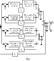 figure 19.36 (a) Sliding-mode controller block diagram; (b) linear control hierarchy for the 12-pulse rectifier. Instead, the slow and fast manifold approach is selected. For the fast manifold, four internal current control loops guarantee the same dc current level in each three-phase rectifier and hmit the short-circuit currents. For the output slow dynamics, an external cascaded output voltage control loop (Fig. 19.36b), measuring the voltage applied to the load, is the minimum. For a straightforward design, given the much slower dynamics of the capacitor voltages compared to the input current, the PI current controllers are calculated as shown in Example 19.6, considering the capacitor voltage constant during a switching period, and = 1 Q the intrinsic resistance of the transformer windings, overlap, and inductor /. From (19.45), = l/r = 0.044 s. From (19.48), with the common assumptions, Tp = 0.0066 s (p = 3). These values guarantee a smaU overshoot (5%) and a current rise time of approximately T/3. To design the external output voltage-control loop, each current-controlled rectifier can be considered a voltage-controlled current source ij.(5)/4, since each half-wave rectifier current response wiU be much faster than the filter output voltage response. Therefore, in the equivalent circuit of Fig. 19.35b, the current source iis) substitutes the input inductor, yielding the transfer function {s)/ii (5): ibXs) CCmRs + C1L252 + (C2R0 + CiR,)s + 1 (19.110) Given the real pole (pi = -6.7) and two complex poles (P23 =-6.65 lb j 140.9) of (19.110), the PI voltage controller zero (1/T=pi) can be chosen with a value equal to the transfer function real pole. The integral gain Tp can be determined using a root-locus analysis to determine the maximum gain, that still guarantees the stability of the closed loop controlled system. The critical gain for the PI was found to be Tzv/Tpv 0.4, then Tp > 0.37. The value T, 2 was selected to obtain weak oscillations, together with almost no overshoot. The dynamic and steady-state responses of the output currents of the four rectifiers (ij, ц^, ц^, ц^) and the output voltage were analyzed using a step input from 2 A to 2.5 A applied at t = 1.1 s, for the currents, and from 40 V to 50 V for the v voltage. The PI current controllers (Fig. 19.37) show good sharing of the total current, a slight overshoot (( = 0.7) and response time 6.6 ms (T/p). The open-loop voltage v presents a rise time of 0.38 s. The PI voltage controller (Fig. 19.38) shows a response time of 0.4 s no overshoot. The four three-phase half-wave rectifier output currents (ij, ц^, i, and ii) present nearly the same transient and steady-state values, with no very high current peaks. These results vahdate the assumptions made in the PI design. The closed-loop performance of the fixed-frequency sliding-mode controller (Fig. 19.39), shows that all the \ \ \ \ currents are almost equal and have peak values only slightly higher than those obtained with the PI linear controllers. The output voltage presents a much faster response time (150 ms) than the PI linear controllers, negligible or no steady-state error, and no overshoot. From these waveforms it can be concluded that the sliding-mode controller provides a much more effective control of the rectifier, as the output voltage response time is much lower than the obtained with PI linear controUers, without significantly increasing the 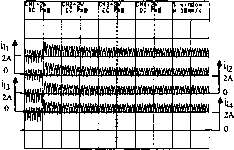 t(50ms/div)-► a) ill, /2 /3? /4 closed loop currents VcjCV) 50- 40--30--20-. 10--0 -
t (lOOms/div) - b) open-loop output voltage v figure 19.37 pi current controller performance.
2A 0 2A 0 1 112 2A 414 2A 0 t (50ras/div) - a) /1, ii2y Ua closed loop currents 60V 40V 20V 0 <C2 20V 0 t(100ms/div)-► b) closed output voltage vand e output voltage error figure 19.38 pi voltage controller performance. thyristor currents, overshoots, or costs. Furthermore, sliding mode is an elegant way to know the variables to be measured, and to design aU the controller and the modulator electronics. Example 19.13. Sliding-Mode Control of Pulse Width Modulation Audio Power Amplifiers. Linear audio power amplifiers can be astonishing, but have efficiencies as low as 15-20% with speech or music signals. To improve the efficiency of audio systems while preserving the quality, PWM switching power amplifiers, enabling the reduction of the power-supply cost, volume, and weight and compensating the efficiency loss of modern loudspeakers, are needed. Moreover, PWM amphfiers can provide a complete digital solution for audio power processing. 2A 0 2A 0 Ч 2A 0 2A 0 t (50ms/div) - c2r VC2 60V t (50ms/div) - (a) (b) figure 19.39 Closed-loop constant-frequency sliding-mode controller performance. For high-fidelity systems, PWM audio amplifiers must present flat passbands of at least 16Hz-20kHz (±0.05 dB), distortions less than 0.1% at the rated output power, fast dynamic response, and signal-to-noise ratios above 90 dB. This requires fast power semiconductors (usually MOSFET transistors), capable of switching at frequencies near 500 kHz and fast nonlinear control methods to provide the precise and timely control actions needed to accomplish the mentioned requirements and to ehminate the phase delays in the LC output filter and in the loudspeakers. A low-cost PWM audio power amplifier, able to provide over SOW to 8-Q loads (V = 50 V), can be obtained using a half-bridge power inverter (switching at fpM 450 kHz), coupled to an output filter for high-frequency attenuation (Fig. 19.40). A low-sensitivity, doubly terminated passive ladder (double LC), low-pass filter using fourth-order Chebyshev approximation polynomials is selected, given its ability to meet, while minimizing the number of inductors, the foUowing requirements: passband edge frequency 21kHz, pass-band ripple 0.5 dB, stopband edge frequency 300 kHz, and 90 dB minimum attenuation in the stopband (Li=80iH l2 = 85iH; Q = 1.7 iF; c2 = 82 nF; = 8 Q; ri = 0.47 Q). Modeling the PWM Audio Amplifier The two half-bridge switches must always be in complementary states, to avoid power supply internal short circuits. Their state can be represented by the time-dependent variable 7, which is 7 = 1 when Ql is on and Q2 is off, and is 7 = - 1 when Ql is off and Q2 is on. Neglecting switch delays, on state semiconductor voltage drops, auxihary networks, and supposing smaU dead times, the half-bridge output voltage is PWM = ydd- Considering the state variables and circuit components shown in Fig. 19.40, and modehng the loudspeaker load as a perturbation represented by the current (ensuring robustness against the frequency l7 1 Speaker \\ -Jc2№ FIGURE 19.40 PWM audio amplifier with fourth-order Chebyshev low-pass output filter and loudspeaker load. dependent impedance of the speaker), the switched state-space model of the PWM audio amplifier is l/Q 0 0 1/Li 0 0 0 -1/l2 0 0 0 0 -1/c2j -1/Q 0 1/c2 yVdd in -1/l2 (19.111) This model wiU be used to define the output voltage controUer. Sliding-Mode Control of the PWM Audio Amplifier The filter output voltage divided by the amplifier gain (1 Cy) must follow a reference . Defining the output error as e = v, - kv and also using its time derivatives (60, бу, e) as a new state vector e = [e, Cq, ву, e], the system equations, in the phase canonical (or controUabUity) form, can be written in the form - [e, ее, ву, ef = [eg, ву, e, -f(e, ее, ву, e) + Pe(t)-yVdd/CiLiC2L2f (19.112) Sliding-mode control of the output voltage wiU enable a robust and reduced order dynamics, independent of semiconductors, power supply, and filter and load parameters. According to (19.75) and (19.112), the sliding surface is S(e,,ee,ey,ef,t) = % + keCe + кубу + /с^е^ = v, - Kv, + ke- d [d{v - k,vj dt[-df- . d [d fd(v,-k,v,)\ di[di[ di ) (19.113) In sliding mode, (19.113) confirms the amplifier gain (0/0, = /K)- To obtain a stable system and the smallest possible response time t, a pole placement according to a third-order Bessel polynomial is used. Taking t inversely proportional to a frequency just below the lowest cut-off frequency (ш^) of the double LC filter (t, 2.8/Ш1 2.8/(2я 21 kHz) 20 is) and using (19.72c) with m = 3, the characteristic polynomial (19.114), verifying the Routh-Hurwitz criterion, is obtained S(e, 5) = 1 + st,+{stf+(st,f (19.114) From (19.91) the switching law for the control input at time tjt, 7(tjt), must be 7(tfc) = sgn{S(e, tfc) + esgn[S(e, t i)]] (19.115) To ensure reaching and existence conditions, the power supply voltage Vj must be greater than the maximum required mean value of the output voltage in a switching period Vjj > (tpwMmax)- The shding-mode controller (Fig. 19.41) is obtained from (19.113), (19.114), and (19.115) with kg = t ky = 62/15, /c = t/l5. The derivatives can be approximated by the block diagram of Fig. 19.41b, were h is the oversampling period. Figure 19.42a shows the ipvwvf o, o/l and the error 10 X (v, - v,/lO) waveforms for a 20-kFiz sine input. The overall behavior is much better than the obtained with the sigma-delta controllers (Figs. 19.43 and 19.44) explained below for comparison purposes. There is no 0.5-dB loss or phase delay over the entire audio band; the Chebyshev filter behaves as a maximally flat filter, with higher stopband attenuation. Figure 19.42b shows ipvwvf o, and 10 x (v, - v,/10) with a 1-kFiz square input. There is almost no steady-state error and almost no overshoot on the speaker voltage V attesting to the speed of response (t20is as designed, since, in contrast to Example 19.12, no derivatives were neglected). The stability, the system order reduction, and the shding-mode controller usefulness for the PWM audio amphfier are also shown. Sigma Deha Controlled PWM Audio Amplifier Assume now the fourth-order Chebyshev low-pass filter, as an ideal filter removing the high-frequency content of the Vpm voltage. Then, the Vp voltage can be vor-kv vc (e(t)-e(M))tr/l4>g kteta (e(t)-e(t-1)H Hysterisis gama epsilon comparator (e (t)-e (t-1))tr/h kbeta a) in 1 1/z J Sum6 tr/h out 1 Unit Delay b) figure 19.41 (a) Sliding-mode controller for the PWM audio amplifier; (b) implementation of the derivative blocks. 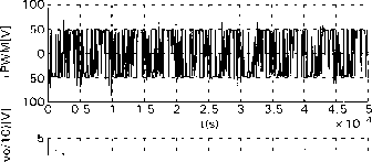 0 0.5 1 1.5 2 2.5 3 t{s) 4.5 5 xlO-4 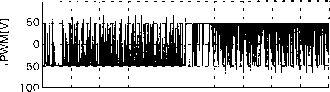 > 6 о 0 0.1 0.2 0.3 0.4 0.5 0 tis) 3 6 0.7 0.8 0.9 1 xlO-3 0 0.1 0.2 0.3 0.4 0.5 0.6 0.7 0.8 0.9 1 t(s) xlO figure 19.42 Sliding-mode controlled audio power amplifier performance (upper graphs show > Vpjj; lower graphs traces 1 show (v = v, lower graphs traces 2 show >i;/10, and lower graphs trace 3 show 10 x {v - y/lO)), (a) response to a 20-kHz sine input, at 55 W output power; (b) response to 1 kHz square-wave input, at 100 W output power. vpwmr t 1/s Sum4 kvvpwm integr Hysteresis gama epsilon comparator +-2 fPWM integ Hysteresis gama gain epsiion comparator figure 19.43 (a) First-order sigma-delta modulator; (b) second-order sigma-delta modulator. considered the amphfier output. However, the discontinuous voltage VpM = ydd is not a state variable and cannot foUow the almost continuous reference ipvwvf The new error variable epvvf = pwm - Kydd is always far from the zero value. Given this nonzero error, the approach outlined in Section 19.3.4 can be used. The switching law remains (19.115), but the new control law (19.116) is vPWM ,t) = K (vpwM,-Kyydd)<t = 0 (19.116) The к parameter is calculated to impose the maximum switching frequency fp- Since /с Jo (tPWM, + kV)dt = 2e, we obtain fpwM = <PWM, + К (19.117) Assuming that ipvwvf, is nearly constant over the switching period l/fpwM (19.116) confirms the amplifier gain, since = VpMjk,. Practical implementation of this control strategy can be done using an integrator with gain к (к 1800), and a comparator with hysterisis г(г 6 mV), Fig. 19.43a. Such an arrangement is caUed a first-order sigma delta (Zzl) modulator. Figure 19.44a shows the Vp, v,, and v,/10 waveforms for a 20-kHz sine input. The overaU behavior is as expected, because the practical filter and loudspeaker are not ideal, but notice the 0.5-dB loss and phase delay of the speaker voltage v mainly due to the output filter and speaker inductance. In Fig. 19.44b, the ipvwvf o, i;/10, and error 10 x (i; - v,/10) for a 1-kHz square input are shown. Note the osciUations and steady-state error of the speaker voltage v due to the filter dynamics and double termination. A second-order sigma-delta modulator is a better compromise between circuit complexity and signal-to-quantization noise ratio. As the switching frequency of the two power MOSFET (Fig. 19.40) cannot be further increased, the second-order structure named cascaded integrators with feedback (Fig. 19.43b) was selected, and designed to eliminate the step response overshoot found in Fig. 19.44b. Figure 19.45b, for 1-kHz square input, shows much less overshoot and osciUations than Fig. 19.44b. However, the ipvwvf o, о/Ю waveforms for a 20-kHz sine input presented in Fig. 19.45a show increased output voltage loss, compared to the first-order sigma-delta modulator, since the second-order modulator was designed to eliminate the output voltage ringing (therefore reducing the amplifier band- 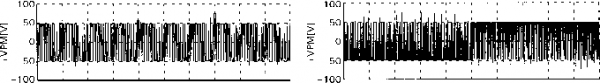 0 0.1 0.2 0.3 0.4 0.5 0.6 0.7 0.8 0.9 1 t(s) xlO 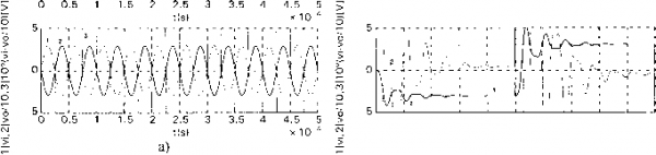 0 0.1 0.2 0.3 0.4 0.5 0.6 0.7 0.8 0.9 1 t(s) xlO figure 19.44 First-order sigma delta audio amplifier performance (upper graphs Vpjj; lower graphs trace 1, {v = Vi); trace 2, v/lO; and trace 3, 10 X (i; - (a) response to 20-kHz sine input, at 55 W output power; (b) response to 1 kHz square wave input, at 100 W output power. lOOr 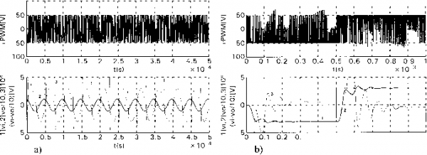 3 0.4 0.5 0.6 0.7 0.8 0.9 1 t{s) xlO FIGURE 19.45 Second-order sigma delta audio amplifier performance (upper graphs Vp,; lower graphs trace 1, (i; = v); lower graphs trace 2, Vq/10; and lower graphs trace 3, 10 x (v - v/lO)); (a) response to a 20-kHz sine input, at 55 W output power; (b) response to 1-kHz square wave input, at 100 W output power. width). The obtained performances with these and other sigma-deha structures are inferior to the shding-mode performances (Fig. 19.43). Shding mode brings definite advantages as the system order is reduced, flatter pass-bands are obtained, power supply rejection ratio is increased, and the nonlinear effects, together with the frequency-dependent phase delays, are cancelled out. Example 19.14. Sliding-Mode Control of Near-Unity Power-Factor PWM Rectifiers. Boost-type voltage-sourced three-phase rectifiers (Fig. 19.46) are multiple-input, multiple-output (MIMO) systems capable of bidirectional power flow, near unity power factor operation, and almost sinusoidal input currents, and can behave as ac-dc power supplies or power factor compensators. The fast power semiconductors used (usually MOSFETs or IGBTs), can switch at frequencies much higher than the mains frequency, enabling the voltage controller to provide an output voltage with fast dynamic response. Modeling the PWM Boost Rectifier Neglecting switch delays and dead times, the states of the switches of the kth inverter leg (Fig. 19.46) can be represented by the time dependent nonlinear variables y, defined as 1 if Зщ is on and Sl is off 0 if Зщ is off and Sl is on (19.118) Consider the displayed variables of the circuit (Fig. 19.46), where L is the value of the boost inductors, R their resistance, С the value of the output capacitor, and R its equivalent series resistance (ESR). Neglecting semiconductor voltage drops, leakage currents, and auxiliary networks, the application of Kirchhoff laws (taking the load current as a time-dependent perturbation) yields the following switched state-space model of the boost rectifier:
-2?! +72 +Уз 3L -2У2 + у3+У1 3L -R -273 + 71 + 72 0 0 0 TA zl L L L L С 0 0 0 FIGURE 19.46 Voltage sourced pwm rectifier with IGBTs and test load. dt (19.119) 470 where .1 RR,\ (I RR, 1 RR, -Щ(у1(у1 - у2) + у2(у2 Уз) + Гз(Уз Tl)) 3L Since the input voltage sources have no neutral connection, the preceding model can be simphfied, eliminating one equation. Using the relationship (19.120) between the fixed fi-ames Xi 2 and x i, in (19.119), the state space model (19.121), in the a-P fi-ame, is obtained V273 0 -7T76 ущ (19.120) -R 0 -R -Уц At, A\ 32 y,R, yR, -1 С (19.121) where /1 iiA , RR, A?3 = Shding-Mode Control of the PWM Rectifier The model (19.121) is nonlinear and time variant. Applying the Park transformation (19.122), using a frequency со rotating reference frame synchronized with the mains (with the q component of the supply d Jt cos(cot) - sin(a;t) sin(a;t) cos(a;t) -R -yd (19.122) - CD L -R -yq L L Ad Ad Ad 31 32 33 Г 1 ycjRc Увс -1 LI L с dtJ (19.123) where A-y( И?Л , /1 RR, -RM + yl) This state-space model can be used to obtain the feedback controllers for the PWM boost rectifier. Considering the output voltage Vg and the current as the controlled outputs and y, the control inputs (MIMO system), the input-output linearization of (19.123), gives the state-space equations in the controllability canonical form (19.124): de dt R + Rc(y] + yl) у] + у1 --L- -L ydVd + yqVq Rip /1 RRc\di LC \C L ) dt 1 RR, (19.124) vohages equal to zero), the nonlinear, time-invariant model (19.123) is written: 19 Control Methods for Power Converters where Using the rectifier overall power balance (fi-om Tellegen s theorem, the converter is conservative, e.g. the power delivered to the load or dissipated in the converter parasitic elements equals the input power), and neglecting the switching and output capacitor losses, dd + qq = 00 + Щ' Supposing Unity power factor (iq 0), and the output in steady state, TdU + yqk d = VyRMS q = 0 7 q/o y{v-Ri)/v,. Then, from (19.124) and (19.75), the following two sliding surfaces can be derived: Sie,-, t) = kAL, - L) = 0
L-CRR,4bYpMS-R4 - Ч = Ч -d = (19.126) where is the time constant of the desired first-order response of output voltage i; ( > T > 0). For the synthesis of the closed-loop control system, notice that the terms of (19.126) inside the square brackets can be assumed as the reference current . Furthermore, from (19.125) and (19.126) it is seen that current control loops for and are needed. Considering (19.122) and (19.120), the two sliding surfaces can be written SM,t) = i-i, = 0 (19.127a) Sp(e,, t) = - = 0 (19.127b) The switching laws relating the sliding surfaces (19.127) with the switching variables are If 5,(\, t)> 8 then z; > hence choose y to increase the current If a,p(\f, 0 < -e then 4 < 4 hence choose y to decrease the current (19.128) The practical implementation of this switching strategy could be accomphshed using three independent two-level hysteresis comparators. Fiowever, this might introduce limit cycles as only two line currents are independent. Therefore, the control laws (19.127) can be implemented using the block diagram of Fig. 19.47a, with d,q-a,P (from (19.122)) and 1,2-а,5 (from (19.120)) transformations and two three-level hysteretic comparators with equivalent hysterisis г and p to limit the maximum switching frequency. A limiter is included to bound the i reference current to ijmax keeping the input line currents within a safe value. This helps to eliminate the nonminimum-phase behavior (outside sliding mode) when large transients are present, while providing short-circuit-proof operation. a- Space Vector Current Modulator Depending on the values of y, the bridge rectifier leg output voltages can assume only eight possible distinct states represented as voltage vectors in the a- reference frame (Fig. 19.47b), for sources with isolated neutral. With only two independent currents, two three-level hysterisis comparators, for the current errors, must be used in order to accurately select all eight available voltage vectors. Each three-level comparator can be obtained by summing the outputs of two comparators with two levels each. One of these two comparators (Siq, dif) has a wide hysterisis width and the other {d, df) has a narrower hysterisis width. The hysterisis bands are represented by 8 and p. Table 19.2 represents all possible output combinations of the resulting four two-level Space vector decoder & driver 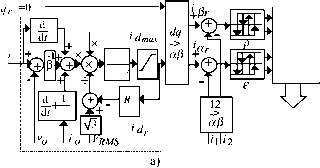 To power switches 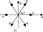 TABLE 19.2 Two-level and three-level comparator results, showing corresponding vector choice, corresponding and vector component voltages. Vectors are mapped in Fig. 19.47b
comparators, their sums giving the two three-level comparators (q ), plus the voltage vector needed to accomplish the current tracking strategy ( - 4) = 0 (ensuring (4 - 4) X (4 - z;,)/dt < 0), plus the variables and the a- voltage components. From the analysis of the PWM boost rectifier it is concluded that, if, for example, the voltage vector 2 is applied (7 = 1, 72 = Ь 7з = 0)пп boost operation, the currents 4 and wiU both decrease. Oppositely, if the voltage vector 5 (7 = 0, 72 = 0, 73 = 1) is apphed, the currents 4 and will both increase. Therefore, vector 2 should be selected when both and currents are above their respective references, that is for = - 1, Sp = -1, whereas vector 5 must be chosen when both and currents are under their respective references, or for = 1, = 1. Nearly aU the outputs of Table 19.2 can be fiUed using this kind of reasoning. The cases where 3 = 0, = - 1, the vector is selected upon the value of the current error (if > 0 and S < 0 then vector 2, if S < 0 and S < 0 then vector 3). When = 0, Sf = 1, if La > 0 Na < then vcctor 6, clsc if < 0 and Na > 0 then vector 5. The vectors 0 and 7 are selected in order to minimize the switching frequency (if two of the three upper switches are on, then vector 7, otherwise vector 0). The space vector decoder can be stored in a look-up table (or in an EPROM) whose inputs are the four two level comparator outputs and the logic result of the operations needed to select between vectors 0 and 7. PI Output Vohage Control of the Current-Mode PWM Rectifier Using the (X-P current mode hysteresis modulators to enforce the and currents to foUow their reference values, , i (the values of L and С are such that the and iq currents usually exhibit a very fast dynamics compared to the slow dynamics of v,), a first-order model (19.129) of the rectifier output voltage can be obtained from (19.124). К(у] + у1) Rc , , 4 ( 19 129) Assuming now a pure resistor load Ri = v,/i and a mean delay between the i current and the reference , continuous transfer functions result for the i current (ij = (1 + sTj) ) and for the v, voltage {v, = kjid/i} + sk) with /c and k obtained from (19.129). Therefore, using the same approach as Examples 19.6, 19.8, and 19.11, a linear PI regulator, with gains Kp and Щ (19.130), sampling the error between the output voltage reference v, and the output v can be designed to provide a voltage proportional {kj) to the reference current i (i = (Kp + KJs)kj{v, - v,)). Ri + Rc Rciy] + yl) (19.130) K,=- 1 RR 1 ... 44 45 46 47 48 49 50 ... 91 |
||||||||||||||||||||||||||||||||||||||||||||||||||||||||||||||||||||||||||||||||||||||||||||||||||||||||||||||||||||||||||||||||||||||||||||||||||||||||||||||||||||||||||||||||||||||||||||||||||||||||||||||||||||||||||||||||||||||||||||||||||||||||||||||||||||||||||||||||||||||||||||||||||||||||||||||||||||||||||||||||||||||||||||||||||||||||||||||||||||||||||||||||||||||||||||||||||||||||||||||||||||||||||||||||||||||||||||||||||||||||||||||||||||||||||||||||||||||||||||||||||||||||||||||||||||||||||||||||||||||||||||||||||||||||||||||||||||||||||||||||||||||||||||||||||||||||||||||||||||||||||||||||||||||||||||||||||||||||||||
|
© 2026 AutoElektrix.ru
Частичное копирование материалов разрешено при условии активной ссылки |