 |
 |
 |
| Главная Журналы Популярное Audi - почему их так назвали? Как появилась марка Bmw? Откуда появился Lexus? Достижения и устремления Mercedes-Benz Первые модели Chevrolet Электромобиль Nissan Leaf |
Главная » Журналы » Metal oxide semiconductor 1 ... 45 46 47 48 49 50 51 ... 91 These PI regulator parameters depend on the load resistance Ri, on the rectifier parameters (C, R, L, R), on the rectifier operating point 7 on the mean delay Тф and on the required damping factor C. Therefore, the expected response can only be obtained with nominal load and input voltages, the line current dynamics depending on the Kp and gains. Results (Fig. 19.48) obtained with the values Ll.lmH, iO.lQ, C 2000 F equivalent series resistance ESR 0.1 Q I] = 0.0012, Vrms70V, with 0.1 Q), ii25Q, i212Q, Kp = 1.2, Ki = 100, kj = 1, show that the a- space vector current modulator ensures the current tracking needed (Fig. 19.48). The step response reveals a faster sliding-mode controUer and the correct design of the current mode/PI controller parameters. The robustness property of the shding-mode controUed output v compared to the current mode/PI, is shown in Fig. 19.49. Example 19.15. Sliding-Mode Controllers for multilevel Inverters. Muhilevel inverters (Fig. 19.50) are the converters of choice for high-voltage, high-power dc-ac or ac-ac (with dc link) applications, as the active semiconductors (usually gate turn-off thyristors (GTO), or IGBT transistors) of n-level power conversion systems, must withstand only a fraction (normally UJ{n - 1)) of the total supply voltage U. Moreover, the output voltage of multilevel converters, being staircase-like waveforms with n steps, features lower harmonic distortion compared to the two-level waveforms with the same switching frequency. The advantages of multUevel converters are paid into the price of the capacitor supply voltage dividers (Fig. 19.51) and voltage equalization circuits, or into the cost of extra power supply arrangements (Fig. 19.51c). This example shows how to extend the two-level switching law (19.81) to /7-level converters, and how to equalize the voltage of the capacitive dividers. 20 10 S 0 -10 -20 AO -50.  0.01 0.02 0.03 tls] 0.04 0.05 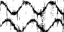 FIGURE 19.48 a- space vector current modulator operation at near unity power factor; (a) simulation result (z + 30; + 30; 2 x /2 - 30; (b) experimental result (1 z, 2 Z2 (10 A/div); 3 z, 4 Z2 (5 A/div)). 0 M.VA- 0.005 0.01 0.02 0.025 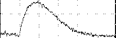 0.005 0.01 0.02 0.025 t [s] t [s] Ю - r [V] with sliding mode control b) - r [V] with current mode/PI control FIGURE 19.49 Transition from rectifier to inverter operation (z from 8 A to -8 A) obtained by switching off IGBT Sa and using 4 = 16 A (Fig. 19.46). Load Ucc-и 2
S33 П AC \ Load j FIGURE 19.50 (a) Single phase, neutral-clamped, three-level inverter with IGBTs; (b) three-phase, neutral-clamped, three-level inverter. Considering single-phase three level inverters (Fig. 19.50a), open-loop control of the output voltage can be made using three-level SWPWM. The two-level modulator, seen in Example 19.9, can be easily extended (Fig. 19.52a) to generate the ущ command (Fig. 19.52b) to three-level inverter legs, from the two-level 7jj signal, using the following relation: 7lII - 7lI(mi,sin(cof)-sgn(m,sin(cof))/2-r(f)/2) - 1/2 + sgn(m sin(a;t))/2 (19.131) The required three-level SWPWM modulators for the output voltage synthesis seldom take into account the semiconductors and the capacitor voltage divider nonideal characteristics. Consequently, the capacitor voltage divider tends to drift, one capacitor being overcharged, the other discharged, and an asymmetry appears in the currents of the power supply. A steady-state error in the output voltage can also be present. Sliding-mode control can provide the optimum switching timing between aU the converter levels, together with robustness to supply voltage disturbances, semiconductor nonidealities, and load parameters. Sliding-Mode Switching Law For a variable-structure system where the control input Ui(t) can present n levels, consider the n values of the integer variable 7, being -(n - I)/2 < у < (n - 1)/2 and Ui(t) = yU /(n - 1), dependent on the topology and on the conducting semiconductors. To ensure the sliding-mode manifold invariance condition (19.76) and the reaching mode behavior, the switching strategy y(t]i) for the time instant t, considering the value of y(t) must be y(t) + 1 if S(e., t) > г л S(e., t) > eA7(tfc) < (n-l)/2 (19.132) 7(tfc)-l if S(e, t) <-8 A S(e, t) < -8 A 7(tfc) > -(n - l)/2 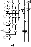 Hrs8 > I I I---It narll i 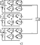 FIGURE 19.51 (a) Five-level {n = 5) diode clamped inverter with IGBTs; (b) five-level {n = 5) flying capacitor converter; (c) multilevel converter based on cascaded full bridge inverters. Modulation Index Product2 Sine №ve (PU) r(t) PU Relay S4 Hysteriss 10-5 High outut=0.5 Low output=-0.5 gamalll 0.5*8gn ► 0>>- Gain FIGURE 19.52 (a) Three-level SWPWM modulator schematic; (b) main three-level SWPWM signals. 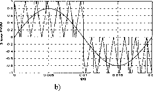 S(exi.t) -epsi-t-eps out:+1-1 >Ju/clt>- f(u) (u[iru[2]>0)* dS/dt -eps;+eps out:+1-1 ±(n-1)/£ gama Memory S(exi.t -1.3eps;+1.3eps out>0.5,+0.5 -1.2eps;+1.2eps out>0.5,+0.5 -eps;+eps out:-0.5,+0.5 -1.1eps;+1.1eps out:-0.5,+0.5 gama decoder FIGURE 19.53 (a) Multilevel sliding-mode PWM modulator with -level hysteresis comparator of quantization interval e; (b) a four hysterisis comparator implementation of a five-level switching law. This switching law can be implemented as depicted in Fig. 19.53. Control of the Output Voltage in Single-Phase Multilevel Converters To control the inverter output voltage, in a closed loop, in diode-clamped multilevel inverters with n levels and supply voltage (7, a control law similar to (19.116), S(e,, t) = KJ(u,-kMUJ(n-l))dt = 0, is suitable. Figure 19.54a shows the waveforms of a five-level sliding-mode controlled inverter, namely the input sinus voltage, the generated output staircase wave, and the sliding-surface instantaneous error. This error is always within a band centered around the zero value and presents zero mean value, which is not the case of 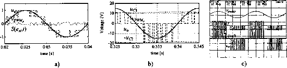 FIGURE 19.54 (a) Scaled waveforms of a five-level sliding-mode controlled single-phase converter, showing the input sinus voltage Vp, the generated output staircase wave u, and the value of the sliding surface S(ei, t); (b) scaled waveforms of a three-level neutral-point clamped inverter showing the capacitor voltage unbalance (shown as two near flat lines touching the tips of the PWM pulses); (c) experimental results from a laboratory prototype of a three-level single-phase power inverter with the capacitor voltage equalization described. 1 -vpwmr kvvpwm Sum4 integr gama n level hysterisis comparator LU int Sum4 gama n level hysterisis comparator kc-(uc2-Ucc/2) kc*(uc2-Ucc/2) figure 19.55 (a) Multilevel sliding-mode output voltage controller and PWM modulator with capacitor voltage equalization; (b) Sliding-mode output current controller with capacitor voltage equalization. 2000 -2000  1 0 0.01 0.02 0.03 0.04 time [s] 0.05 0 0.01 0.02 0.03 0.04 0.05 time [s] 0 0.01 0.02 0.03 0.04 0.05 time [s] figure 19.56 Simulated performance of a five-level power inverter, with a U voltage dip (from 2kV to 1.5 kV). Response to a sinusoidal wave of frequency 50 Hz. (a) Vpjj input; (b) PWM output voltage u; (c) the integral of the error voltage, which is maintained close to zero. sigma-delta modulators foUowed by n-level quantizers, where the error presents an offset mean value in each half period. Experimental multilevel converters always show capacitor voltage imbalances (Fig. 19.54b) due to smaU differences between semiconductor voltage drops and circuitry offsets. To obtain capacitor voltage equalization, the voltage error (v, - U,J2) is fed back to the controller (Fig. 19.55a) to counteract the circuitry offsets. Experimental results (Fig. 19.54c) clearly show the effectiveness of the correction made. The smaU steady-state error between the voltages of the two capacitors still present could be eliminated using an integral regulator (Fig. 19.55b). Figure 19.56 confirms the robustness of the sliding-mode controller to power supply disturbances. Output Current Control in Single-Phase Multilevel Converters Considering an inductive load with current ii, the control law (19.91) and switching law (19.132), should be used for single-phase multilevel inverters. Results obtained using the capacitor voltage equahzation principle just described are shown in Fig. 19.57. Example 19.16. Sliding-Mode Controllers for Three-Phase Multilevel Inverters. Three-phase n-level inverters (Fig. 19.58) are suitable for high-voltage, high-power dc-ac applications, such as modern highspeed railway traction drives, as the controUed turn-off semiconductors must block only a fraction (normally Udc/(n - 1)) of the total supply voltage Uc- 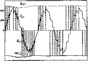 -200 -400 -600 0.005 0.01 0.015 0.02 0.025 0.03 0.035 0.04 0.045 0.05 time[s) figure 19.57 Operation of a three-level neutral-point clamped inverter as a sinusoidal current source: Scaled waveforms of the output current sine wave reference , the output current z, showing ripple, together with the PWM-generated voltage tz, with nearly equal pulse heights, corresponding to the equalized dc capacitor voltages U(i and U(2- 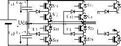 S33 Us3 figure 19.58 Three-phase, neutral-clamped three-level inverter with IGBTs. This example presents a realtime modulator for the control of the three output voltages and capacitor voltage equalization, based on the use of sliding mode and space vectors represented in the otj] frame. Capacitor voltage equalization is done with the proper selection of redundant space vectors. Output Voltage Control in Multilevel Converters For each leg of the three-phase multilevel converter, the switching strategy for the к leg (/cG {1,2,3}) must ensure complementary states to switches S]i and З^з. The same restriction must be observed for 5;2 4. Neglecting switch delays, dead times, on-state semiconductor voltage drops, snubber networks, amd power-supply variations, supposing small dead times and equal capacitor voltages, and using the time-dependent switching variable y](t), the leg output voltage Щ (Fig. 19.58) will be Щ = y{t)UJ2, with 7(0 = 1 if Sjti л Sjt2 are ON л A S are OFF 0 if Sjt2 Л Sjt3 are ON л Si л 5;4 are OFF - 1 if Sjt3 Л Sjt4 are ON л S л 5;2 OFF (19.133) The converter output voltages U] of vector U5 can be expressed 2/3 -1/3 -1/3 -1/3 2/3 -1/3 -1/3 -1/3 2/3 (19.134) The apphcation of the Concordia transformation Usi,2,3 = и sa,,a (19.135) to (19.134) reduces the number of equations Us, Us, Us, 1 0 i/лД -1/2 V3/2 1/V2 (19.135) The output voltage vector in the coordinates Vsr is г 2 JLbj (19.136) 211211 Ь=\уъ-\УХ-\У2 (19.137) The output voltage vector in the coordinates U, is discontinuous. A suitable state variable for this output can be its average value U during one switching period: Uc dt = 4 r -dt (19.138) The controUable canonical form is T 2 (19.139) Considering the control goal U = Uj and (19.75) the sliding surface is = k ,A(V.-Us.,) (Us ,.f-Us ,)d = 0 (19.140) To ensure reaching mode behavior, and sliding mode stability (19.76), as the first derivative of (19.140), S(eo , t), is S(e ,t)=(U,-U,J the switching law is (19.141) S(e , 0 > 0 S(e , t) < 0 U > U, S(e , 0 < 0 S(e , t) > 0 U < U, (19.142) This switching strategy must select the proper values of U from the avaUable outputs. As each inverter leg (Fig. 19.58) can deliver one of three possible output voltages ((7j/2; 0; -UJ2), aU the 27 possible output voltage vectors listed in Table 19.3, can be represented in the aP frame of Fig. 19.59 (in per units, 1 p.u. = U). There are nine different levels for the a space vector component and only five for the P component. Fiowever, considering any particular value of a (or P) component, there are at most five levels available in the remaining orthogonal component. From the load view- point, the 27 space vectors of Table 19.3 define only 19 distinct space positions (Fig. 19.59). To select one of these 19 positions from the control law (19.140) and the switching law (19.142), two five-level hysteretic comparators (Fig. 19.53b) must be used (5 = 25). Their outputs are the integer variables 1 and Я^, denoted Я^ (Я^, (Я^ g {-2; -1; 0; 1; 2}) corresponding to the five selectable levels of Г^, and Г^. Considering sliding-mode stability, Я^,, at time step j + 1, is given by (19.143), knowing their previous values at step j. This means that the output level is increased (decreased) if the error and its derivative are both positive (negative), provided the maximum (minimum) output level is not exceeded. (а,);+1 = (a,); + 1 if S(e, t) > 8 AS(e, 0>гл(Я^Д-<2 = (Kf)j - 1 if S(e, t) < -8 AS(ep,t) < -гл(Я^Д- > -2 (19.143) The available space vectors must be chosen not only to reduce the mean output voltage errors, but also to guarantee transitions only between adjacent levels, to *0,8 -0, 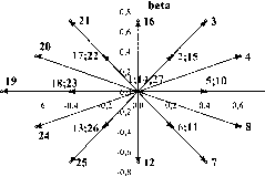 9 alfa 0,8 1,0 FIGURE 19.59 Output voltage vectors (1 to 27) of three-phase, neutral-clamped three-level inverters, in the frame. minimize the capacitor voltage unbalance, to minimize the switching frequency, to observe minimum on or off times if apphcable, and to equally stress aU the semiconductors. Using (19.143) and the control laws S(e, t) (19.140), Tables 19.4 and 19.5 can be used to choose the correct voltage vector in order to ensure stability, current tracking, and capacitor voltage equalization. The vector with a, components corresponding to the levels of the pair Я^, 1 is selected, provided that adjacent TABLE 19.3 Vectors of the three-phase three-level converter, switching variables y, switch states Sj and the corresponding output voltages, line to neutral point, line to line, and components in per units
TABLE 19.4 Switching Table for Current Control and ui > u2 the Inverter Mode, or ui < u2 the Regenerative Mode ((U(ji - U(j2) (TiZi + T2Z2) > 0), Showing Vector Selectioin upon the Variable Я^,
transitions on inverter legs are obtained. If there is no directly corresponding vector, then the nearest vector guaranteeing adjacent transitions is selected. If more than one vector is the nearest, one is selected to equalize the capacitor voltages. One of the three vectors (1, 14, 27) corresponding to the zero vector is selected to minimize the switching frequency. The discrete values of Я^, allow 25 different combinations. As only 19 are distinct from the load viewpoint, the extra ones can be used to select vectors able to equalize the capacitor voltages. From circuit analysis it can be seen that vectors {2, 5, 6, 13, 17, 18} result in the discharge of capacitor Cp if the inverter is operating in Ъ Levfil f!oTiveFteii 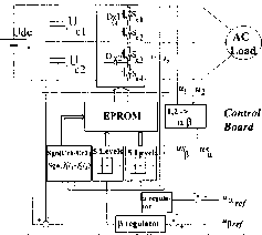 the inverter mode, or in the discharge of if the inverter is operating as a boost rectifier. Similar reasoning can be applied for vectors {10, 11, 15, 22, 23, 26} and capacitor C2. Therefore, considering the vector 2 = [(7i,2/2)(7i,2 + 1) - (7з/2)(7з + 1)] if (ci 02) x(Tiz\ + T2i2) > 0, then according to Я^,, choose one of the vectors {2,5,6, 13, 17, 18} (Table 19.4). If (Uqi - 112) Cih + 2h) < 0 then according to Я^,, choose one of the vectors {10, 11, 15, 22, 23, 26} (Table 19.5). As an example, consider the case where > (72-Then the capacitor C2 must be charged and Table 19.4 must be used if the multilevel inverter is operating in the inverter mode or Table 19.5 for the regenerative mode. Addicionally, when using Table 19.4, if Я^, = - 1 and Я^ = -1, then vector 13 should be used. Experimental results shown in Fig. 19.61 were obtained with a low-power, low-voltage laboratory prototype (150 V, 3kW) of a three-level inverter (Fig. 19.60), controlled by two four-level comparators, plus described capacitor voltage equalizing procedures and EPROM-based lookup Tables 19.3, 19.4 and 19.5. Transistors IGBT (MG25Q2YS40) were switched at frequencies near 4-kFiz, with neutral clamp diodes 40FiFL, Ci C2 20 mF. The load was mainly inductive (3 X 10 mH, 2Q). The inverter number of levels (three for the phase voltage and five for the line voltage), together with the adjacent transitions of inverter legs between levels, are shown in Fig. 19.61a) and, in detail, in Fig. 19.62a). The performance of the capacitor voltage equahzing strategy is shown in Fig. 19.62b, where the reference current of phase 1 and the output current of phase 3, together with the power supply voltage (U 100V) and the voltage of capacitor C2 (/2), can be seen. It can be noted that the U(j2 voltage is nearly half of the supply voltage. Therefore, the capacitor voltages are nearly equal. Furthermore, it can be stated that without this voltage equalization procedure, the three-level inverter operates only during a brief transient, during which one of the capacitor voltages vanishes to nearly zero volts and the other is overcharged to the supply voltage. Figure 19.61b shows the harmonic spectrum of the output voltages, where the harmonics due to the switching frequency (4.5 kFiz) and the fundamental harmonic can be seen. On-line Output Current Control in Multilevel Inverters Considering a standard inductive balanced load (R, L) with electromotive force {u) and isolated neutral, the converter output currents can be expressed FIGURE 19.60 Block diagram of the multilevel converter and control board. (19.144) CH1S50V CH2S50V CH4=20mV 2nfis/div 11Шп11Н111  a) b) FIGURE 19.61 (a) Experimental results showing phase and line voltages; (b) Harmonic spectrum of output voltages. Now analysing the circuit of Fig. 19.58, the multilevel converter switched state-space model can be obtained: The application of the Concordia matrix (19.135) to (19.145), reduces the number of the new model (19.146) equations to two, since an isolated neutral is assumed d Jt
Щ Щ L% J (19.145) d Jt 0 lA 0 0 - (19.146) The model (19.146) of this multiple-input, multiple-output system (MIMO) with outputs 4, ь reveals the control inputs Ui variables y](t). (7, dependent on the control stopped 1999/11/26 20:37:07 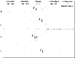
FIGURE 19.62 Experimental results showing (a) the transitions between adjacent voltage levels (50 V/div; time 20 /xs/div); (b) performance of the capacitor voltage equalizing strategy; from top trace to bottom: 1, the voltage reference input; 2, the power supply voltage; 3, the midpoint capacitor voltage, which is maintained close to t/j/2; 4, the output current of phase 3 (2A/div; 50 V/div; 20ms/div). From (19.146) and (19.75), the two sliding surfaces (af,t) are S(e , t) = kakpref - = = 0 (19-147) The first derivatives of (19.146), denoted S(eo,, t), are: S(eo , 0 = k(i -i) (19.148) Therefore, the switching law is S(e , 0 > 0 S(e , 0 < 0 S(e , 0 < 0 S(e , 0 > 0 (19.149) These switching laws are implemented using the same aP vector modulator described above in this example. Figure 19.63a shows experimental results. The multilevel converter and proposed control behavior are obtained for step inputs (2 A to 4 A) in the amplitude of the sinus references with frequency near 52 Fiz (Uj50V). Observe the tracking ability, the fast transient response, and the balanced three phase currents. Figure 19.63b shows almost the same test (step response from 4 A to 2 A at the same frequency). but now the power supply is set at 150 V and the inductive load was unbalanced (±30% of resistor value). The response remains virtually the same, with tracking ability, no current distortions due to dead times or semiconductor voltage drops. These results confirm experimentally that the designed controllers are robust concerning these nonidealities. 19.4 Fuzzy Logic Control of Power Converters 19.4.1 Introduction Fuzzy logic control [17,18,19] is a heuristic approach that easily embeds the knowledge and key elements of human thinking in the design of nonlinear controllers. Qualitative and heuristic considerations, which cannot be handled by conventional control theory, can be used for control purposes in a systematic form by applying fuzzy control concepts [3]. Fuzzy logic control does not need an accurate mathematical model, can work with imprecise inputs, can handle nonhnearity, and can present disturbance insensitivity greater than most nonhnear controllers. Fuzzy logic controllers usually outperform other controllers in complex, nonlinear, or undefined systems for which a good practical knowledge exists. Fuzzy logic controUers are based on fuzzy sets, i.e., classes of objects in which the transition from membership to nonmem-bership is smooth rather than abrupt. Therefore, boundaries of fuzzy sets can be vague and ambiguous, making them useful for approximation systems. stopped 1999/11/20 17:39:43 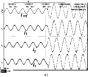 Stopped 1999/11/20 17:51:13
FIGURE 19.63 Step response of the current control method; (a) step from 2 A to 4 A in the reference amplitude at 52 Hz. Traces show the reference current for phase 1 and the three output currents with 50 V power supply; (b) Step from 4 A to 2 A amplitude. Traces show the reference current for phase 1 and the three output currents with 150 V power supply (5 A/div; time scale 20ms/div). The first step in the fuzzy controller synthesis procedure is to define the input and output variables of the fuzzy controUer. This is done accordingly with the expected function of the controller. There are not any general rules to select those variables, although typically the variables chosen are the states of the controlled system, their errors, error variation, and/or error accumulation. In power converters, the fuzzy controUer input variables are commonly the output voltage or current error, and/or the variation or accumulation of this error. The output variables u(k) of the fuzzy controUer can define the converter duty cycle (Fig. 19.6), or a reference current to be apphed in an inner current mode PI or sliding-mode controUer. The fuzzy controUer rules are usually formulated in linguistic terms. Thus, the use of linguistic variables and fuzzy sets implies the fuzzification procedure, e.g. the mapping of the input variables into suitable linguistics values. Rule evaluation or decision-making infers, using an inference engine, the fuzzy control action from the knowledge of the fuzzy rules and the linguistic variable definition. The output of a fuzzy controUer is a fuzzy set, and thus it is necessary to perform a defuzzification procedure, e.g. the conversion of the inferred fuzzy result to a nonfuzzy (crisp) control action, that better represents the fuzzy one. This last step obtains the crisp value for the controller output u(k) (Fig. 19.64). These steps can be implemented on-hne or off-line. On-line implementation, useful if an adaptive controUer is intended, performs realtime inference to obtain the controller output and needs a fast enough processor. Off-hne implementation employs a lookup table built according to the set of aU possible combinations of input variables. To obtain this lookup table, input values in a quantified range are converted (fuzzification) into fuzzy variables (linguistic). The fuzzy set output, obtained by the inference or decision-making engine according to linguistic control rules (designed by the expert knowledge), is then converted into numeric controUer output values (defuzzification). The table contains the output for aU the combinations of quantified input entries. Off-hne process can actually reduce the controUer actuation time since the only effort is limited to consulting the table at each iteration. This section presents the main steps for the implementation of a fuzzy controUer suitable for power converter control. A meaningful example is provided. r(k) e(k) 7 FUZZY CONTROLLER Rule Base \u{k)
Data Base FIGURE 19.64 Structure of a fuzzy logic controller. 19.4.2 Fuzzy Logic Controller Synthesis Fuzzy logic controUers consider neither the parameters of the power converter or their fluctuations, nor the operating conditions, but only the experimental knowledge of the power converter dynamics. In this way, such a controller can be used with a wide diversity of power converters implying only smaU modifications. The necessary fuzzy rules are simply obtained considering roughly the knowledge of the power converter dynamic behavior. 19.4.2.1 Fuzzification Assume, as fuzzy controUer input variables, an output voltage (or current) error, and the variation of this error. For the output, assume a signal u{k), the reference input of the converter. 19.4.2.1.1 Quantization Levels Consider the reference r(k) of the converter output kth sample, y(k). The tracking error e(k) is e(k) = r(k) - y(k) and the output error change Ak), between the samples к and к - 1, is determined by Ak) = е{к)-е{к-1). These variables and the fuzzy controUer output u(k), usually ranging from - lOV to lOV, can be quantified in m levels {-(m - l)/2, +(m - l)/2}. For off-line implementation, m sets a compromise between the finite length of a lookup table and the required precision. 19.4.2.1.2 Linguistic Variables and Fuzzy Sets The fuzzy sets for Xg, the linguistic variable corresponding to the error e(k), for xg, the hnguistic variable corresponding to the error variation A(k), and for the linguistic variable of the fuzzy controUer output u(k), are usually defined as positive big (PB), positive medium (PM), positive smaU (PS), zero (ZE), negative smaU (NS), negative medium (NM), and negative big (NB), instead of having numerical values. In most cases, the use of these seven fuzzy sets is the best compromise between accuracy and computational task. 19.4.2.1.3 Membership Functions A fuzzy subset, for example Si(Si = (NB, NM, NS, ZE, PS, PM, or PB)) of a universe £, coUection of e(k) values denoted generically by {e}, is characterized by a membership function ju: E [0, 1], associating with each element e of universe E, a number iiie) in the interval [0,1], which represents the grade of membership of e to E. Therefore, each variable is assigned a membership grade to each fuzzy set, based on a corresponding membership function (Fig. 19.65). Considering the m quantization levels, the membership function fii(e) of the element e in the universe of discourse £, may take one of the discrete values included in si() {0; 0.2; 0.4; 0.6; 0.8; 1; 0.8; 0.6; 0.4; 0.2; 0}. Membership functions are stored in the database (Fig. 19.64). Considering e(k) = 2 and Ae(k) = -3, taking into account the staircase-like membership functions defined in Fig. 19.65, 1 ... 45 46 47 48 49 50 51 ... 91 |
|||||||||||||||||||||||||||||||||||||||||||||||||||||||||||||||||||||||||||||||||||||||||||||||||||||||||||||||||||||||||||||||||||||||||||||||||||||||||||||||||||||||||||||||||||||||||||||||||||||||||||||||||||||||||||||||||||||||||||||||||||||||||||||||||||||||||||||||||||||||||||||||||||||||||||||||||||||||||||||||||||||||||||||||||||||||||||||||||||||||||||||||||||||||||||||||||||||||||||||||||||||||||||||||||||||||||||||||||||||||||||||||||||||||||||||||||||||||||||||||||||||||||||||||||||||||||||||||||||||||||||||||||||||||||||||||||||||||||||||||||||||||||||||||||||||||||||||||||||||||||||||||||||||||||||||||||||||||||||||||||||||||||||||||||||||||||||||||||||||||||||||||||||||||||||||||||||||||||||||||||||||||||||||||||||||||||||||||||||||||||||||||||||||||||||||||||||||||||||||||||||||||||||||||||||||||||||||||||||||||||||||||||||||||||||||||||||||||||||||||||||||||||||||||||||||||||||||||||||||||||||||||||||||||||||||||||||||||||||||||
|
© 2026 AutoElektrix.ru
Частичное копирование материалов разрешено при условии активной ссылки |