 |
 |
 |
| Главная Журналы Популярное Audi - почему их так назвали? Как появилась марка Bmw? Откуда появился Lexus? Достижения и устремления Mercedes-Benz Первые модели Chevrolet Электромобиль Nissan Leaf |
Главная » Журналы » Metal oxide semiconductor 1 ... 46 47 48 49 50 51 52 ... 91 NB NM NS ZE PS PM PB -20 -15 -10 -5 0 5 10 15 20 FIGURE 19.65 Membership functions in the universe of discourse. it can be said that is PS and also ZE, being equally PS and ZE. Also, is NS and ZE; being less ZE than NS. 19,4,2,1,4 Linguistic Control Rules The generic linguistic control rule has the following form: If хД) is membership of the set Sj = (NB, NM, NS, ZE, PS, PM, or PB) AND х^Д) is membership of the set Sj = (NB, NM, NS, ZE, PS, PM, or PB), THEN the output control variable is membership of the set S = (NB, NM, NS, ZE, PS, PM, or PB). Usually, the rules are obtained considering the most common dynamic behavior of power converters, the second-order system with damped oscillating response (Fig. 19.66). Analyzing the error and its variation, together with the rough linguistic knowledge of the needed control input, an expert can obtain linguistic control rules such as the ones displayed in Table 19.6. For example, at point 6 of Fig. 19.66 the rule is if xXk) is NM AND x,(/c) is ZE, THEN x(k + 1) should be NM. Table 19.6, for example, states that: if xXk) is NB AND x,(/c) is NB, THEN x(k + 1) must be NB, or if xXk) is PS AND x,(/c) is NS, THEN x(k + 1) must be NS, or if xXk) is PS AND x,(/c) is ZE, THEN x(k + 1) must be PS, or if xXk) is ZE AND x,(/c) is NS, THEN x(k + 1) must be NS, or if xXk) is ZE AND x,(/c) is ZE, THEN x(k + 1) must be ZE, or if... These rules (rule base) alone do not allow the definition of the control output, as several of them may apply at the same time. 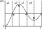 FIGURE 19.66 Reference dynamic model of power converters: second-order damped oscillating error response. 19.4.2.2 Inference Engine The result of a fuzzy control algorithm can be obtained using the control rules of Table 19.6, the membership functions, and an inference engine. In fact, any quantified value for e(k) and Ak) is often included into two linguistic variables. With the membership functions used, and knowing that the controUer considers e(k) and A e(k), the control decision generically must be taken according to four linguistic control rules. To obtain the corresponding fuzzy set, the min-max inference method can be used. The minimum operator describes the AND present in each of the four rules, that is, it calculates the minimum between the discrete value of the membership function li(xXk)) and the discrete value of the membership function 1л^(х^(к)). The THEN statement links this minimum to the membership function of the output variable. The membership function of the output variable wiU therefore include trapezoids limited by the segment mm(fi(xXk)), fisjiAei- The OR operator linking the different rules is implemented by calculating the maximum of aU the (usually four) rules. This mechanism to obtain the resulting membership function of the output variable is represented in Fig. 19.67. 19.4.2.3 Defuzzification As shown, the inference method provides a resulting membership function sj.(m()) the output fuzzy variable (Fig. 19.67). Using a defuzzification process, this final membership function, obtained by combining aU the membership functions, as a consequence of each rule, is then converted into a numerical value, called u(k). The defuzzification strategy can TABLE 19.6 Lingquistic control rules Rule 1: if : is Positive Small and x Ae is Zero then result is Positive Small Rule 2: if xe is; Zero and x д e i$ Negative Small then result is Negative Small . NS хе=Ъ ZE PS then result NM NS X де=-4 NM resulting membership function NM NS A ZE PS FIGURE 19.67 Application of the min-max operator to obtain the output membership function. be the center of area (COA) method. This method generates one output value u{k), which is the abscissa of the gravity center of the resulting membership function area, given by the foUowing relation: (19.150) This method provides good results for output control. Indeed, for a weak variation of e(k) and A(k), the center of the area wiU move just a little, and so does the controUer output value. By comparison, the alternative defuzzification method, the mean of maximum strategy (MOM), is advantageous for fast response, but it causes a greater steady-state error and overshoot (considering no perturbations). 19.4.2.4 Lookup Table Construction Using the rules given in Table 19.6, the min-max inference procedure, and COA defuzzification, aU the controUer output values for aU quantified e(k) and A(k) can be stored in an array to serve as the decision lookup table. This lookup table usually has a three-dimensional representation simUar to Fig. 19.68. A microprocessor-based control algorithm just picks up output values from the lookup table. Example 19.17. Fuzzy Logic Control of Unity Power Factor Buck-Boost Rectifiers. Consider the near unity power factor buck-boost rectifier of Fig. 19.69. 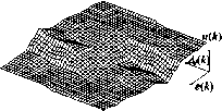 FIGURE 19.68 Three-dimensional view of the lookup table. The switched state space model of this converter can be written dVCf Rf. 1 1 1 . Ур . c/-c/ (19.151) 0 where 1, (switch 1 and 4 are ON) and (switch 2 and 3 are OFF) 0, all the switches are OFF -1, (switch 2 and 3 are ON) and (switch 1 and 4 are OFF) 1, 0, For comparison purposes, a PI output voltage controller is designed considering that a current mode PWM modulator enforces the reference value for the current (which usually exhibits a fast dynamics compared with the dynamics of Vq. A first-order model, simUar to (19.129) is obtained. The PI gains are similar to (19.100) and load dependent (Kp = C,/(2T), K = 1/(2W). A fuzzy controUer is obtained considering the approach outlined, with seven membership functions for the output voltage error, five for its change, and three membership functions for the output. The linguistic control rules are obtained as the ones depicted in Table 19.6 and the lookup table is simUar to Fig. 19.68. Performances obtained for the step response show a fuzzy controUed rectifier behavior close to the PI behavior. The advantages of the fuzzy controUer emerge for perturbed loads or power supplies, where the low sensitivity of the fuzzy controUer to system parameters is clearly seen (Fig. 19.70). Therefore, fuzzy controUers are advantageous for power converters with changing loads or supply voltage values and other external disturbances. 19.5 Conclusions Control techniques for power converters were reviewed. Linear controUers based on state-space averaged models or circuits is Lf,Rf IGBTlN ЮВТЗ  IGBT2 IGBT4 FIGURE 19.69 Unity power factor buck-boost rectifier with 4 IGBTs. are weU estabhshed and suitable for the apphcation of hnear systems control theory. Obtained hnear controllers are useful, if the converter operating point is almost constant and disturbances are not relevant. For changing operating points and strong disturbances, linear controllers can be enhanced with nonlinear, antiwindup, soft-start, or saturation techniques. Current-mode control wiU also help to overcome the main drawbacks of linear controllers. Sliding mode is a nonlinear approach weU adapted for the variable structure of the power converters. The critical problem of obtaining the correct sliding surface was highlighted, and examples were given. The sliding-mode control law allows the implementation of the power converter controller, and the switching law gives the PWM modulator. The system variables to be measured and fed back are identified. The obtained reduced order dynamics is not dependent on system parameters or power supply (as long as it is high enough), presents no steady-state errors, and has a faster response speed (compared with linear controllers), as the system order is reduced and nonidealities are ehminated. Should the measure of the state variables be difficult, state observers may be used, with steady-state errors easily corrected. Sliding-mode controUers provide robustness against bounded disturbances and an elegant way to obtain the controller and modulator, using just the same theoretical approach. Fixed-frequency operation was addressed and solved, together with short-circuit-proof operation. Presented fixed-frequency techniques were applied to converters that can only operate with fixed frequency. Sliding-mode techniques were successfully applied to multiple-input multiple-output power converters and to multUevel converters, solving the capacitor voltage divider equalization. Sliding-mode control needs more information from the controUed system than do linear controllers, but is probably the most adequate tool to solve the control problem of power converters. Fuzzy logic controller synthesis was briefly presented. Fuzzy logic controllers are based on human experience and intuition and do not depend on system parameters or operating points. Fuzzy logic controUers can be easily applied to various types of power converters having the same qualitative dynamics. Fuzzy logic controUers, like sliding-mode controllers, show robustness against load and power supply perturbations, semiconductor nonidealities (such as switch delays or uneven conduction voltage drops), and dead times. The controUer implementation is simple, if based on the off-hne concept. On-line implementation requires a fast microprocessor but  0.2 0.25 0.3 0.35 0.4 0.45 0.5 0.55 0.6 0.65 0.7 Time [s] I I I 0.2 0.25 0.3 0.35 0.4 0.45 0.5 0.55 0.6 0.65 0.7 nme[s] a) b) FIGURE 19.70 Simulated result of the output voltage response to load disturbances {R = 50 Q to i? = 150 Q at time 0.3 s); (a) PI control; b) fuzzy logic control. can include adaptive techniques to optimize the rule base and/ or the database. Acknowledgments The author thanks aU the researchers whose works contributed to this chapter, namely S. Pinto, V. Pires, J. Quadrado, T. Amaral, M. Crisostomo, J. Costa, N. Rodrigues and the suggestions of M. P. Kazhierkowski. References 1. B. K. Bose, Power Electronics and AC Drives, Prentice-Hall, New Jersey, 1986. 2. H. Biihler, Electronique de Reglage et de Commander Traite Delec-tricite. Vol XV, Editions Georgi, 2nd ed., 1979. 3. A. Candel and G. Langholz, Fuzzy Control Systems, CRC Press, 1994. 4. G. Chryssis, High Frequency Switching Power Supplies, McGraw-Hill, 1984. 5. J. Fernando Silva, Electronica Industrial, Funda9ao Calouste Gulben-kian, Lisboa, 1998. 6. J. D. Irwin, ed.. The Industrial Electronics Handbook, CRC/IEEE Press, 1996. 7. J. Kassakian, M. Schlecht, and G. Verghese, Principles of Power Electronics, Addison Wesley, 1992. 8. F. Labrique and J. Santana, Electronica de Potencia, Fundagao Calouste Gulbenkian, Lisboa, 199L 9. W. S. Levine, ed.. The Control Handbook, CRC/IEEE Press, 1996. 10. N. Mohan, T. M. Undeland, and W. B. Robins, Power Electronics: Converters, Applications and Design, 2nd ed., John Wiley & Sons, 1995. 11. K. Ogata, Modern Control Engineering, 3rd ed., Prentice-Hall International, 1997. 12. M. Rashid, Power Electronics: Circuits, Devices and Applications, 2nd ed., Prentice-Hall International, 1993. 13. K. K. Sum, Switched Mode Power Conversion, Marcel Dekker Inc., 1984. 14. K. Thorborg, Power Electronics, Prentice-Hall, 1988. 15. V. I. Utkin, Sliding Modes and Their application on Variable Structure Systems, MIR Publishers Moscow, 1978. 16. V. I. Utkin, Sliding Modes in Control Optimization, Springer Verlag, 1981. 17. L. A. Zadeh, Fuzzy Sets, Information and Control 8, 338-353 (1965). 18. L. A. Zadeh, Outline of a New Approach to the Analysis of Complex Systems and Decision Process, IEEE Trans. Syst Man Cybern. SMC-3, 28-44, (1973). 19. H. J. Zimmermann, Fuzzy Sets: Theory and Its Applications, Kluwer-Nijhoff, 1995. Power Supplies Y. M. Lai, Ph.D. Department of Electronic and Information Engineering The Hong Kong Polytechnic University Hung Нот, Hong Kong 20.1 20.2 20.3 20.4 20.5 Introduction...................................................................................... 487 Linear Series Voltage Regulator............................................................. 488 20.2.1 Regulating Control 20.2.2 Current Limiting and Overload Protection Linear Shunt Voltage Regulator............................................................. 491 Integrated Circuit Voltage Regulators..................................................... 492 20.4.1 Fixed Positive and Negative Linear Voltage Regulators 20.4.2 Adjustable Positive and Negative Linear Voltage Regulators 20.4.3 Applications of Linear 1С Voltage Regulators Switching Regulators........................................................................... 494 20.5.1 Single-Ended Isolated Flyback Regulators 20.5.2 Single-Ended Isolated Forward Regulators 20.5.3 Half-Bridge Regulators 20.5.4 Full-Bridge Regulators References......................................................................................... 506 20.1 Introduction Power supplies are used in most electrical equipment. Their apphcations cut across a wide spectrum of product types, ranging from consumer appliances to industrial utilities, from miUiwatts to megawatts, from hand-held tools to sateUite communications. By definition, a power supply is a device that converts the output from an ac power line to a steady dc output or multiple outputs. The ac voltage is first rectified to provide a pulsating dc, and then filtered to produce a smooth voltage. Finally, the voltage is regulated to produce a constant output level despite variations in the ac line voltage or circuit loading. Figure 20.1 illustrates the process of rectification, filtering, and regulation in a dc power supply. The transformer, rectifier, and filtering circuits are discussed in other chapters. In this chapter, we wiU concentrate on the operation and characteristics of the regulator stage of a dc power supply. In general, the regulator stage of a dc power supply consists of a feedback circuit, a stable reference voltage, and a control circuit to drive a pass element (a sohd-state device such as transistor or MOSFET). The regulation is done by sensing variations appearing at the output of the dc power supply. A control signal is produced to drive the pass element to cancel any variation. As a result, the output of the dc power supply is maintained essentially constant. In a transistor regulator, the pass element is a transistor, which can be operated in its active region or as a switch, to regulate the output voltage. When the transistor operates at any point in its active region, the regulator is referred to as a linear voltage regulator. When the transistor operates only at cutoff and at saturation, the circuit is referred to as a switching regulator. Linear voltage regulators can be further classified as either series or shunt types. In a series regulator, the pass transistor is connected in series with the load as shown in Fig. 20.2. Regulation is achieved by sensing a portion of the output voltage through the voltage divider network Ri and R2, and comparing this voltage with the reference voltage Vp to produce a resulting error signal that is used to control the conduction of the pass transistor. This way, the voltage drop across the pass transistor is varied and the output voltage delivered to the load circuit is maintained essentially constant. In the shunt regulator shown in Fig. 20.3, the pass transistor is connected in paraUel with the load, and a voltage-dropping resistor is connected in series with the load. Regulation is achieved by controUing the current conduction of the pass transistor such that the current through R remains essentially constant. This way, the current through the pass transistor is varied and the voltage across the load remains constant. As opposed to hnear voltage regulators, switching regulators employ solid-state devices, which operate as switches, either completely on or completely ojf, to perform power conversion. Because the switching devices are not required to operate in their active regions, switching regulators enjoy a much lower power loss than those of linear voltage regulators. Figure 20.4 FIGURE 20.1 Block diagram of a dc power supply. FIGURE 20.2 A linear series voltage regulator. shows a switching regulator in a simphfied form. The high-frequency switch converts the unregulated dc voltage from one level to another dc level at an adjustable duty cycle. The output of the dc supply is regulated by means of a feedback control that employs a pulse-width modulator (PWM) controller, where the control voltage is used to adjust the duty cycle of the switch. Both linear and switching regulators are capable of performing the same function of converting an unregulated input into a regulated output. However, these two types of regulators have significant differences in properties and performances. In designing power supphes, the choice of using certain type of regulator in a particular design is significantly based on the cost and performance of the regulator itself. In order to use the more appropriate regulator type in the design, it is necessary to understand the requirements of the application and select the type of regulator that best satisfies those requirements. Advantages and disadvantages of linear regulators, as compared to switching regulators, are given below: 1. Linear regulators exhibit efficiency of 20 to 60%, whereas switching regulators have a much higher efficiency, typically 70 to 95%. 2. Linear regulators can only be used as a step-down regulator, whereas switching regulators can be used in both step-up and step-down operations. 3. Linear regulators require a mains-frequency transformer for off-the-hne operation. Therefore, they are heavy and bulky. On the other hand, switching regulators use high-frequency transformers and can therefore be smaU in size. 4. Linear regulators generate little or no electrical noise at their outputs, whereas switching regulators may produce considerable noise if they are not properly designed. 5. Linear regulators are more suitable for applications of less than 20 W, whereas switching regulators are more suitable for large power apphcations. In this chapter, we wiU examine the circuit operation, characteristics, and applications of linear and switching regulators. In Section 20.2, we wiU look at the basic circuits and properties of linear series voltage regulators. Some current-limiting techniques wiU be explained. In Section 20.3, linear shunt regulators wiU be covered. The important characteristics and uses of hnear 1С regulators will be discussed in Section 20.4. Finally, the operation and characteristics of switching regulators wiU be discussed in Section 20.5. Important design guidelines for switching regulators wiU also be given in this section. 20.2 Linear Series Voltage Regulator A Zener diode regulator can maintain a fairly constant voltage across a load resistor. It can be used to improve the voltage regulation and reduce the ripple in a power supply. However, the regulation is poor and the efficiency is low because of the nonzero resistance in the Zener diode. To improve the regulation and efficiency of the regulator, we have to limit the Zener current to a smaller value. This can be accomplished by using an amplifier in series with the load as shown in Fig. 20.5. The effect of this amphfier is to limit the variations of current through the Zener diode. This circuit is known as a hnear series voltage regulator because the transistor is in series with the load. Because of the current-amplifying properties of the transistor, the current in the Zener diode is reduced by a factor of + 1). Fience there is a little voltage drop across the diode resistance and the Zener diode approximates an ideal voltage source. The output voltage V, of the regulator is (20.1) The change in output voltage is AV, = AV, + AVbe (20.2) where is the dynamic resistance of the Zener diode and is the output resistance of the transistor. Assume that and are constant. With AI, Ali/(P + 1), the change in output voltage is then AV, Al,r, (20.3) If Vl is not constant, then the current / wiU change with the input voltage. When the change in output voltage is calculated, this current change must be absorbed by the Zener diode. In designing linear series voltage regulators, it is imperative that the series transistor work within the rated SOA and be protected from excess heat dissipation because of current overloads. The emitter to coUector vohage Ve of is given by VcE = У г - У о (20.4) Thus, with specified output voltage, the maximum allowable Vqe for a given is determined by the maximum input voltage to the regulator. The power dissipated by can be approximated by Consequently, the maximum aUowable power dissipated in is determined by the combination of the input voltage and the load current Ip of the regulator. For a low output voltage and a high loading current regulator, the power dissipated in the series transistor is about 50% of the power delivered to the output. In many high-current, high-voltage regulator circuits, it is necessary to use a Darhngton-connected transistor pair so that the voltage, current, and power ratings of the series element are not exceeded. The method is shown in Fig. 20.6. An additional desirable feature of this circuit is that the reference diode dissipation can be reduced greatly. The maximum base current is then /(/zpi + 1)(р£2 + !) This current is usually of the order of less than 1 mA. Consequently, a low-power reference diode can be used. 20.2.1 Regulating Control The series regulators shown in Figs. 20.5 and 20.6 do not have feedback loops. Although they provide satisfactory performance for many apphcations, their output resistances and ripples cannot be reduced. Figure 20.7 shows an improved form of the series regulator, in which negative feedback is employed to improve the performance. In this circuit, transistors Q3 and Q4 form a single-ended differential amplifier, and the gain of this amplifier is established by P. Fiere is a stable Zener diode reference, biased by R. For higher accuracy, can be replaced by an 1С reference such as the REF series from Burr-Brown. Resistors R and R2 form a voltage divider for output voltage sensing. Finally, transistors and Q2 form a Darlington pair output stage. The operation of the regulator can be explained as foUows. When and Q2 are on, the output voltage increases, and hence the voltage at the base of Q3 also increases. During this time, Q3 is off and Q4 is on. When Уд reaches a level that is equal to the reference voltage У ref the base of Q4, the base-emitter junction of Q3 becomes forward-biased. Some base current wiU divert into the collector of Q3. If the output voltage V, starts to rise above VpEE, Q3 conduction increases to further decrease the conduction of Ql and Q2, which wiU in turn maintain output (20.5) FIGURE 20.5 Basic circuit of a linear series regulator. FIGURE 20.6 A linear series regulator with Darlington-connected amplifier. FIGURE 20.7 An improved form of discrete component series regulator. voltage regulation. Figure 20.8 shows another improved series regulator that uses an operational amphfier (op-amp) to control the conduction of the pass transistor. One of the problems in the design of hnear series voltage regulators is the high-power dissipation in the pass transistors. If an excess load current is drawn, the pass transistor can be quickly damaged or destroyed. In fact, under short-circuit conditions, the voltage across Q2 in Fig. 20.7 wiU be the input voltage Vj, and the current through Q2 will be greater than the rated fuU-load output current. This current will cause to exceed its rated SOA unless the current is reduced. In the next section, some current-limiting techniques will be presented to overcome this problem. normal operation as soon as the overload condition is removed. One of the current-hmiting techniques to prevent current overload, caUed the constant current-limiting method, is shown in Fig. 20.9a. Current-limiting is achieved by the combined action of the components shown inside the dashed line. The voltage developed across the current-limit resistor and the base-to-emitter voltage of current-limit transistor Q3 is proportional to the circuit output current 4. During current overload, 4 reaches a predetermined maximum value that is set by the value of R to cause Q3 to conduct. As Q3 starts to conduct, Q3 shunts a portion of the base current. This action, in turn, decreases and limits to a maximum value 4(max)- Since the base-to-emitter voltage V of Q3 cannot exceed 0.7 V, the voltage across R is held at this value and 4(max) is limited to L(max) 0.7V (20.6) Consequently, the value of the short-circuit current is selected by adjusting the value of R. The voltage-current characteristic of this circuit is shown in Fig. 20.9b. 20.2.2 Current Limiting and Overload Protection In some series voltage regulators, overloading causes permanent damage to the pass transistors. The pass transistors must be kept from excessive power dissipation under current overloads or short-circuit conditions. A current-limiting mechanism must be used to keep the current through the transistors to a safe value as determined by the power rating of the transistors. The mechanism must be able to respond quickly to protect the transistor and yet permit the regulator to return to О Hence, the current required in to maintain the conduction state of Q3 is also decreased. Consequently, as the load resistance is reduced, the output voltage and current faU, and the current-limit point decreases toward a minimum when the output voltage is short-circuited. In summary, any regulator using foldback current-limiting can have peak load current up to 4(niax)- when the output becomes shorted, the current drops to a lower value to prevent overheating of the series transistors. FIGURE 20.10 Voltage-current characteristic of foldback current-limit. In many high-current regulators, foldback current-limiting is always used to protect against excessive current. This technique is similar to constant current-hmiting, except that as the output voltage is reduced as a result of load impedance moving toward zero, the load current is also reduced. Therefore, a series voltage regulator that includes a foldback current-hmiting circuit has the voltage-current characteristic shown in Fig. 20.10. The basic idea of foldback current-limiting, with reference to Fig. 20.11, can be explained as follows. The foldback current-limiting circuit (in dashed outline) is similar to the constant current-limiting circuit, with the exception of resistors R and R. At low output current, the current-limit transistor Q3 is cut off. A voltage proportional to the output current Ip is developed across the current-hmit resistor R. This voltage is apphed to the base of Q3 through the divider network R and R. At the point of transition into current limit, any further increase in wiU increase the voltage across R and hence across R, and Q3 wiU be progressively turned on. As Q3 conducts, it shunts a portion of the base current. This action, in turn, causes the output voltage to fall. As the output voltage faUs, the voltage across R decreases and the current in R also decreases, and more current is shunted into the base of Q3. 20.3 Linear Shunt Voltage Regulator The second type of linear voltage regulator is the shunt regulator. In the basic circuit shown in Fig. 20.12, the pass transistor Ql is connected in paraUel with the load. A voltage-dropping resistor i3 is in series with this paraUel network. The operation of the circuit is simUar to that of the series regulator, except that regulation is achieved by controUing the current through Ql. The operation of the circuit can be explained as foUows. When the output voltage tries to increase because of a change in load resistance, the voltage at the noninverting terminal of the operational amplifier also increases. This voltage is compared with a reference voltage and the resulting difference voltage causes Qi conduction to increase. With constant and V, 4 ill decrease and V, wiU remain constant. The opposite action occurs when V, tries to decrease. The voltage appearing at the base of Qi causes its conduction to decrease. This action offsets the attempted decrease in Vn and maintains it at an almost constant level. Analytically, the current flowing in R is R3 - 01 + h (20.7) (20.8) FIGURE 20.11 Series regulator with foldback current limiting. FIGURE 20.12 Basic circuit of a Hnear shunt regulator. With II and constant, a change in wiU cause a change in (20.9) With Vj- and V constant. A/qi = -Ml (20.10) Equation (20.10) shows that if Iqi increases, 4 decreases, and vice versa. Although shunt regulators are not as efficient as series regulators for most applications, they have the advantage of greater simphcity. This topology offers inherent short-circuit protection. If the output is shorted, the load current is limited by the series resistor R and is given by L(max) (20.11) The power dissipated by can be approximated by 20.4 Integrated Circuit Voltage Regulators The linear series and shunt voltage regulators presented in the previous sections have been developed by various sohd-state device manufacturers and are available in integrated circuit (1С) form. Like discrete voltage regulators, linear 1С voltage regulators maintain an output voltage at a constant value despite variations in load and input voltage. In general, linear 1С voltage regulators are three-terminal devices that provide regulation of a fixed positive voltage, a fixed negative voltage, or an adjustable set voltage. The basic connection of a three-terminal 1С voltage regulator to a load is shown in Fig. 20.14. The 1С regulator has an unregulated input voltage V apphed to the input terminals, a regulated voltage V at the output, and a ground connected to the third terminal. Depending on the selected 1С regulator, the circuit can be operated with load currents ranging from miUiamperes to tens of amperes and output power from milliwatts to tens of watts. Note that the internal construction of 1С voltage regulators may be somewhat more complex and different from that previously described for discrete voltage regulator circuits. However, the external operation is much the same. In this section, some typical linear 1С regulators are presented and their applications are also given. Vole = VMr3 - h) (20.12) For a low value of 4, the power dissipated in is large and the efficiency of the regulator may drop to 10% under this condition. To improve the power handling of the shunt transistor, one or more transistors connected in the common-emitter configuration in paraUel with the load can be employed, as shown in Fig. 20.13. 20.4.1 Fixed Positive and Negative Linear Voltage Regulators The 78XX series of regulators provide fixed regulated voltages from 5 to 24 V. The last two digits of the 1С part number denote the output voltage of the device. For example, a 7824 1С regulator produces a +24 V regulated voltage at the output. The standard configuration of a 78XX fixed positive voltage regulator is shown in Fig. 20.15. The input capacitor Q acts as a line filter to prevent unwanted variations in the input line, and the output capacitor c2 is used to filter the high-frequency noise that may appear at the output. In order to ensure proper operation, the input voltage of the regulator FIGURE 20.13 element. FIGURE 20.14 lator. 1 ... 46 47 48 49 50 51 52 ... 91 |
|
© 2026 AutoElektrix.ru
Частичное копирование материалов разрешено при условии активной ссылки |