 |
 |
 |
| Главная Журналы Популярное Audi - почему их так назвали? Как появилась марка Bmw? Откуда появился Lexus? Достижения и устремления Mercedes-Benz Первые модели Chevrolet Электромобиль Nissan Leaf |
Главная » Журналы » Metal oxide semiconductor 1 2 3 4 5 6 7 8 ... 91 Cathode cathode anode Gate 1  Anode figure 3.19 Cross section of a unit-cell of an emitter switched figure 3.20 Cross-section of a unit-cell of a dual gate emitter thyristor (EST). switched thyristor (DG-EST). that the ITT has a lower forward drop (0.5 V lower at lOOA/cm) with only a slightly increased turn-off time: 0.19 is for the ITT and 0.16 is for the ICBT. The best designed EST is the dual gate emitter switched thyristor (DC-EST) [12]. The structure is shown in Fig. 3.20. The leftmost gate controls the ICBT current, as indicated in the figure. The rightmost gate forms the MOS channel in series with the thyristor current. The second gate determines whether the thyristor section is in or out. Switching as an ICBT has considerable advantages in terms of controllability, particularly in practical circuits. There are a number of important features in the DC-EST. The ICBT section, creating the ICBT electrons is similar to a conventional modern ICBT design. The good shorting essential to latch-up free operation can be identified by the deep p-well along with the cathode metallization. The thyristor structure is unlike that of typical discrete thyristor devices in that the junctions are very shallow, in order to make them compatible with ICBT processing. However, similarities to conventional thyristors exist in that the N2 region must be heavily doped for good electron injection efficiency. Further, in common with conventional thyristors, the P2 region is shorted. Here, the shorting would appear excessive, except that the p-doping is carefully controlled to give a lateral resistance, and unwanted turn-on is not possible as the N2 emitter is separately controlled by its own lateral MOS channel. The DC-EST is intended to be switched in ICBT mode, so as to exploit the controllability and snubberless capabilities of an ICBT. Thus, the lateral MOS channel is only turned on after the voltage across the device has started falling. At turn-off, the lateral MOS channel is turned off a short time before the ICBT section starts to switch. As the lateral MOS only turns off into the ICBT on-state, it needs only a low blocking voltage. Therefore, it can be a good quality lateral device that introduces a low additional voltage in the on-state. 3.6.3 Static Induction Thyristors A static induction thyristor (SITh) or field controlled thyristor (FCTh) has a cross section similar to that shown in Fig. 3.21. Other SITh configurations have surface gate structures. The device is essentially a pin diode with a gate structure that can pinch-off anode current flow. Large area devices are generally the buried-gate type because larger cathode areas and, hence, larger current densities are possible. Planar gate devices have been fabricated with blocking capabilities of up to 1.2 kV and conduction currents of 200 A, while step-gate (trench-gate) structures have been produced that are able to block up to 4kV and conduct 400 A. Similar devices with a Verigrid cathode \\\\\\\\\\\\\ buried gate (p+) anode figure 3.21 Cross section of a static induction thyristor (SITh) or field-controlled thyristor (FCT). Structure have been demonstrated that can block 2kV and conduct 200 A, with claims of up to 3.5-kV blocking and 200-A conduction. Buried gate devices that block 2.5 kV and conduct 300 A have also been fabricated. 3.6.4 Optically Triggered Thyristors Optically gated thyristors have traditionally been used in power utility applications where series stacks of devices are necessary to achieve the high voltages required. Isolation between gate drive circuits for circuits such as static VAR compensators and high-voltage dc to ac inverters have driven the development of this class of devices. One of the most recent devices can block 6kV forward and reverse, conduct 2.5 kA average current, and maintains a di/dt capability of 300 A/is, and a dv/dt capability of 3000 V/is, with a required trigger power of lOmW. An integrated light-triggered and light-quenched static induction thyristor has been produced that can block 1.2 kV and conduct up to 20 A (at a forward drop of 2.5 V). This device is an integration of a normally off, buried-gate static induction photothyristor and a normally off, p-channel Darlington surface-gate static induction photo-transistor. The optical trigger and quenching power required is < 5 and 0.2 mW, respectively. 3.6.5 Bidirectional Control Thyristor The Bidirectional control thyristor (BCT) is an integrated assembly of two antiparallel thyristors on one Si wafer. The intended application for this switch is in VAR compensators, static switches, soft starters, and motor drives. These devices are rated at up to 6.5 kV blocking. Cross talk between the two halves has been minimized. A cross section of the BCT is shown in Fig. 3.22. Note that each surface has a cathode and an anode (opposite devices). The small gate-cathode periphery necessarily restricts the BCT to low-frequency applications because of its di/dt limit. Thyristor half В Separation region Thyristor half A Anode В  Gate A Cathode A Shallow p-base Deep p-base n-base Deep p-base Shallow p-base Cathode В Gate В (not visible) Anode A figure 3.22 Cross section of a bidirectional control thyristor (BCT).  figure 3.23 Cross section and iv plot of a Triac. A low-power device similar to the BCT, but in existence for many years, is the Triac. A simphfied cross section of a Triac is shown in Fig. 3.23. A positive voltage apphed to the anode with respect to the cathode forward-biases /j, while reverse-biasing /2; /4, and /3 are shorted by the metal contacts. When /2 is biased to breakdown, a lateral current flows in the p2-region. This lateral flow forward-biases the edge of /3, causing carrier injection. The result is that the device switches into its thyristor mode and latches. Applying a reverse voltage causes the opposite behavior at each junction, but with the same result. Figure 3.23 also shows the iv plot for a Triac. The addition of a gate connection allows the breakover to be controlled at a lower forward voltage. 3.7 Gate Drive Requirements 3.7.1 Snubber Circuits To protect a thyristor, from a large di/ dt during turn-on and a large dv/dt during turn-off, a snubber circuit is needed. A general snubber topology is shown in Figure 3.24. The turn-on snubber is made by inductance Ц (often Ц is stray inductance only). This protects the thyristor from a large di/dt during the turn-on process. The auxiliary circuit made by and allows the discharging of Ц when the thyristor is turned off. The turn-off snubber is made by resistor R2 and capacitance C2. This circuit protects a СТО from large dv/dt during the turn-off process. The auxiliary circuit made by D2 and R2 allows the discharging of C2 when the thyristor is turned on. The circuit of capacitance C2 and inductance Ц also limits the value of dv/dt across the thyristor during forward blocking. In addition, Ц protects the thyristor from reverse over-currents. 3.7.2 Gate Circuits It is possible to turn on a thyristor by injecting a current pulse into its gate. This process is known as gating the thyristor. The most important restrictions are on the maximum peak and duration of the gate pulse current. In order to allow a safe turn-on commutation, the current pulse should be high Li С figure 3.24 Turn-on (top elements) and turn-off (bottom elements) snubber circuits for thyristors. Gate Voltage T. = -40oC  125 oC Gate Current Minimum Gate Current to Trigger FIGURE 3.25 Gate i-v curve for a typical thyristor. enough and, in order to avoid an unwanted turn-off immediately after the turn-on, it should last for a sufficient time. In estimating how large the gate current pulse should be to ensure device turn on, the gate current-voltage characteristic, which is given with the device data sheet, must be used. An example of this kind of data sheet is shown in Fig. 3.25. In Fig. 3.25 are shown the gate current-voltage characteristics for the maximum and minimum operating temperatures. The dashed line represents the minimum gate current and corresponding gate voltage needed to ensure that the thyristor will be triggered at various operating temperatures. It is also known as the locus of minimum firing points. On the data sheet it is possible to find a line representing the maximum operating power of the thyristor gating internal circuit. The straight line, between Vq and Vq/Rq, represents the current voltage characteristic of the equivalent trigger circuit. If the equivalent trigger circuit line intercepts the two gate current-voltage characteristics for the maximum and minimum operating temperatures after they intercept the dashed line and before they intercept the maximum operating power line, then the trigger circuit is able to turn on the thyristor at any operating temperature without destroying or damaging the device. Another feature of the gating process that should be analyzed is the fast turn-on required for these devices. In order to allow a fast turn-on, and correspondingly large anode di/dt during the turn-on process, a large gate current pulse is supplied during the initial turn-on phase with a large dig/dt. The gate current is kept on, at lower value, for some time after the thyristor is turned on in order to avoid unwanted turn-off  FIGURE 3.26 Gate current waveform showing large initial current followed by a suitable back-porch value. of the device. A shaped gate current waveform of this type is shown in Fig. 3.26. In order to keep the power and control circuits electrically unconnected, the gate signal generator and the gate of the thyristor are often connected through a transformer. There is a transformer winding for each thyristor; this way, unwanted short-circuits between devices are avoided. A general block diagram of a thyristor gate-trigger circuit is shown in Fig. 3.27. This application is for a standard bridge configuration often used in power converters. AC line Voltage Power Converter Input Control Signal DC Power Supply for Current Amplifier Circuit Zero-Crossing Detection and Phase-Angle Circuit OultoT3 Out to T4 Current Amplifier OuttoT2 Qui to Tl  Isolation Transformers for Gate Trigger Signal figure 3.27 Block diagram of a transformer-isolated gate drive circuit. Another problem can arise if the trigger circuit produces just one pulse and there exists an RL-type load. For example, if the circuit is a single-phase controlled bridge, the load is only resistive, and then delay angle between the load current and voltage across is 0°. If the load is an RL-type, the load current will reach zero after the voltage across it does. It could happen that a thyristor is triggered before the opposite one is turned off, and because of the short time of the current pulse, it becomes impossible to control the bridge in the desired way. A possible solution to this problem could be the generation of a longer current pulse. Because of the presence of the transformer, a solution like the one just described is not possible. An alternative solution can be the generation of a series of short pulses that last as long as a long single pulse. A single short pulse, a single long pulse, and a series of short pulses are shown in Fig. 3.28. There are many gate trigger circuits that use optical isolation between the logic-level electronics and a drive stage (typically MOSFETs) configured in a push-pull output. The dc power supply voltage for the drive stage is provided through transformer isolation. Many device manufacturers supply drive circuits available on PC boards or diagrams of suggested circuits. 3.8 PSpice Model Circuit simulators such as Spice and PSpice are widely used as tools in the design of power systems. For this purpose equivalent circuit models for thyristors have been developed. A variety of models have been proposed with varying degrees of complexity and accuracy. Many times the simple two-transistor model described in Section 3.2 is used in PSpice. This simple structure, however, cannot create the appropriate negative-differential-resistance (ndr) behavior as the thyristor moves from forward-blocking to forward-conduction. A -H271; Q n 2n +2% 3n t figure 3.28 Gate pulses used as an alternative to one long current pulse. PSpice model for a GTO developed by Tsay et. al. [13] captures many of the behaviors of thyristors. This model creates device characteristics such as the static I-V curve shown in Fig. 3.3, dynamic characteristics such as turn-on and turn-off times, device failure modes such as current crowding due to excessive di/dt at turn-on, and spurious turn-on due to excessive dv/dt at turn-off, thermal effects, and so on. Specifically, three resistors are added to the two-transistor model to create the appropriate behavior. The proposed two-transistor, three-resistor model (2T-3i) is shown in Fig. 3.29. This circuit exhibits the desired NDR  figure 3.29 GTOs. A two-transistor, three-resistor model for SCRs and behavior. Given the static I-V characteristics for an SCR or GTO, it is possible to obtain similar curves from the model by choosing appropriate values for the three resistors and for the forward current gains and a of the two transistors. The process of curve-fitting can be simplified by keeping in mind that resistor tends to affect the negative slope of the I-V characteristic, resistor R2 tends to affect the value of the holding current 1, and resistor R tends to affect the value of the forward breakdown voltage Vpj. When modeling thyristors with cathode or anode shorts, as described in Section 3.4, the presence of these shorts determines the values of R and R2, respectively. In the case of a GTO an important device characteristic is the so-called turn-off gain K = Ij/\Iq\, that is, the ratio of the anode current to the negative gate current required to turn off the device. An approximate formula relating the turn-off gain to the as of the two transistors is given in what follows: off - a + - 1 (3.3) The ability of this model to predict dynamic effects depends on the dynamics included in the transistor models. If transistor junction capacitances are included, it is possible to model the dv/dt limit of the thyristor. Too high a value of dvj/dt will cause significant current to flow through the /2 junction capacitance. This current acts like a gate current and can turn on the device. -GATE \\ Islands g g VVCathode) Anocje Gate RGCl Cell Model 1 rkck RGC2
RGC8 Cell Model RKC2< RKC3< RKC85
Cathode figure 3.30 Thyristor multicell circuit model containing eight cells. This model does not accurately represent spatial effects such as current crowding at turn-on (the di/dt hmit), when only part of the device is conducting, and, in the case of a GTO, current crowding at turn-off, when current is extracted from the gate to turn off the device. Current crowding is caused by the location of the gate connection with respect to the Load conducting area of the thyristor and by the magnetic field generated by the changing conduction current. Gate-contact and cathode-contact resistance can be included for each cell as well. To model these effects, Tsay et al. [13] propose a multicell circuit model, in which the device is discretized in a number of conducting cells, each having the structure of Fig. 3.30. This model, shown in Fig. 3.31, takes into account the mutual inductive coupling, the delay in the gate turn-off signal due to positions of the cells relative to the gate connection, and nonuniform gate- and cathode-contact resistance. In particular, the RC delay circuits (series R with a shunt С tied to the cathode node) model the time delays between the gate triggering signals due to the position of the cell with respect to the gate connection; coupled inductors, Ms, model magnetic couphng between cells; resistors, Rjcs, model nonuniform contact resistance; resistors, Rqcs, model gate contact resistances. The various circuit elements in the model can be estimated from device geometry and measured electrical characteristics. The choice of the number of cells is table 3.6 Element values for each cell of a multicell GTO model figure 3.31 Single-phase controlled rectifier circuit.
a trade-off between accuracy and complexity. An example of the values of the RC delay network, Rqc, Rkc is given in Table 3.6. 3.9 Applications The most important application of thyristors is for line-frequency, phase-controlled rectifiers. This family includes several topologies, of which one of the most important is used to construct high voltage dc (HVDC) transmission systems. A single-phase controlled rectifier is shown in Fig. 3.31. The presence of thyristors makes the average output voltage controllable by appropriate gating of the thyristors. If the gate signals to the thyristors were continuously applied, the thyristors in Fig. 3.31 behave as diodes. If no gate currents are supplied they behave as open circuits. Gate current can be applied any time (phase delay) after the forward voltage becomes positive. Using this phase-control feature it is possible to produce an average output voltage less than the average output voltage obtained from an uncontrolled rectifier. 3.9.1 Direct current-Alternating current Utility Inverters Three-phase converters can be made in different ways, according to the system in which they are employed. The basic circuit used to construct these topologies is shown in Fig. 3.32. 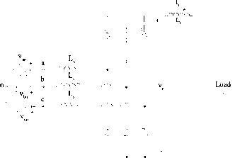 figure 3.32 A 3-phase controlled bridge circuit used as a basic topology for many converter systems. The thyristors in the circuit of Fig. 3.32 are used in the same way they were used in single-phase circuits but necessarily with more complex control. Starting from this basic configuration, it is possible to construct more complex circuits in order to obtain high-voltage or high-current outputs, or just to reduce the output ripple by constructing a multiphase converter. One of the most important systems using the topology shown in Fig. 3.32 as a basic circuit is the HVDC system represented in Fig. 3.33. This system is made by two converters, a transmission line, and two ac systems. Each converter terminal is made of two poles. Each pole is made by connecting two 6-pulse line-frequency converters through ACPowerl Grid #1 Converter #1 rT2-pulse Converter I for Positive Une 12-pulse Converter for Negative Une Filter Filter Converter #2 DC Transmission Lines AC Power Grid #2 figure 3.33 A high-voltage dc (HVDC) transmission system. 2 is 2 AC Grid  i ь Load figure 3.34 Parallel connection of two 6-pulse converters for high-current apphcations. A-Y and 7-7 transformers in order to obtain a 12-pulse converter and a reduced output ripple. The filters are required to reduce the current harmonic generated by the converter. Thyristors are required in order to reduce the voltage amplitude to the ac voltage amplitude level by appropriate switching action. When a large amount of current and relatively low voltage is required, it is possible to connect, using a specially designed inductor, two 6-pulse hne-frequency converters connected through A-Y and 7-7 transformers. This topology is shown in Fig. 3.34. 3.9.2 Motor Control Another important application of thyristors is in motor control circuits. They are used to construct the first stage of an electric motor drive in order to vary the amplitude of the voltage waveform across the windings of the electrical motor as it is shown in Fig. 3.35. An electronic controller controls the gate current of these thyristors. The rectifier and inverter sections can be thyristor circuits. A controlled rectifier is used in conjunction with a square wave or pulse-width modulated (PWM) voltage source inverter (VSI) to create the speed-torque controller system. Figure 3.36 shows a square-wave or PWM VSI with a controlled rectifier on the input side. The switch block inverter is made of thyristors (usually GTOs) for high power. Low-power motor controllers often use IGBT inverters. In motor control, thyristors are also used in current-source inverter (CSI) topologies. When the motor is controlled by a CSI, a controlled rectifier is also needed on the input side. Figure 3.37 shows a typical CSI inverter. Diodes, capacitors, and the motor leakage inductance make a forced commutation circuit. These circuits are needed to force the current through the thyristors to zero, in order to turn them off if using SCRs. This is not needed when using GTOs. This inverter topology does not need any additional circuitry to provide the regenerative braking (energy recovery when slowing the motor). To allow bidirectional power flow. 50 or 60 Hz, 1-Ф огЗ-ф
DC Links  AC Output -Variable Voltage &Variable Frequency figure 3.35 Variable frequency converter for motor control. АС1-Ф or 3-Ф Controlled Rectifier Voltage Single- or Three-phase Inverter  Filter figure 3.36 Pulsewidth modulated or square-wave inverter with a controlled rectifier input.  figure 3.37 Current-source inverter on the output section of a motor drive system using capacitors for power factor correction. then to allow regenerative braking, two back-to-back connected line-fi-equency thyristor converters used to be employed in the past. Use of antiparallel GTOs with symmetric blocking capability or diodes in series with each asymmetric GTO reduces the number of power devices needed, but greatly increases the control complexity. 3.9.3 VAR Compensators and Static Switching Systems Thyristors are also used to switch capacitors (TSC) or inductors (TCI) in order to control the reactive power in the system. An example of these circuits is shown in Fig. 3.38. These circuits act as a static VAR (volts-amps reactive) controller. The topology represented on the left-hand side of Fig. 3.38 is called a thyristor-controlled inductor (TCI) and it acts as a variable inductor where the inductive VAR supplied can be varied quickly. Because the system may require either inductive or capacitive VAR, it is possible to connect a bank of capacitors in parallel with a TCI. The topology shown on the right-hand side of Fig. 3.38 is called a thyristor-switched capacitor (TSC). Capacitors can be switched out by blocking the gate pulse of all thyristors in the circuit. The problem of this topology is the voltage across the capacitors at the thyristor turn-off. At turn-on the thyristor must be gated at the instant of the maximum ac voltage to avoid large over-currents. A less important application of thyristors is as a static transfer switch, used to improve the reliability of uninterruptible power supplies (UPS) as shown in Fig. 3.39. There are two modes of using the thyristors. The first leaves the load permanently connected to the UPS system and in case of emergency disconnects the load from the UPS and connects it directly to the power fine. The second mode is opposite to the first one. Under normal conditions the load is permanently connected to the power fine, and in event of a line outage, the load is disconnected from the power line and connected to the UPS system. 1 2 3 4 5 6 7 8 ... 91 |
|||||||||||||||||||||||||||||||||||||||||||||||||||||||||||
|
© 2026 AutoElektrix.ru
Частичное копирование материалов разрешено при условии активной ссылки |