 |
 |
 |
| Главная Журналы Популярное Audi - почему их так назвали? Как появилась марка Bmw? Откуда появился Lexus? Достижения и устремления Mercedes-Benz Первые модели Chevrolet Электромобиль Nissan Leaf |
Главная » Журналы » Metal oxide semiconductor 1 ... 49 50 51 52 53 54 55 ... 91 Unsuitability for dc applications (emergency lighting, automobile hghting, etc.). 21.2 High-Frequency Supply of Discharge Lamps 21.2.1 General Block Diagram of Electronic Ballasts Figure 21.9 shows the general block diagram of a typical electronic baUast. The main stages are the foUowing: EMI filter. This filter is mandatory for commercial electronic baUasts. Usually it consists of two coupled inductors and a capacitor. The input filter is used to attenuate the electro magnetic interference (EMI) generated by the high-frequency stages of the baUasts. It also protects the baUast against possible hne transients. Ac-dc converter. This stage is used to generate a dc voltage level from the ac line. Normally a fuU-bridge diode rectifier foUowed by a filter capacitor is used. Fiowever, this simple rectifier provides low input power factor and poor voltage regulation. In order to obtain a higher power factor and a regulated bus voltage, active converters can be used, as discussed later in this chapter. Dc-ac inverter and high-frequency ballast. These stages are used to supply the lamp at high frequency. The inverter generates a high-frequency waveform, and the baUast is used to limit the current through the discharge. Both inductors and capacitors can be used to perform this function, with the advantage of low size and weight because they operate at high frequencies. Starting circuit. In most electronic baUasts, especially those for low-pressure discharge lamps, the high-frequency baUast is used to both ignite the lamp and limit the lamp current at steady state. Therefore, no extra starting circuit is necessary. Fiowever, when supplying high-pressure discharge lamps, the starting voltages are much higher and separate ignition circuits are needed, especially if hot reignition is pursued. Control and protection circuit. This stage includes the main osciUator, error amplifiers to regulate lamp current or power, output overvoltage protection, timers to control the ignition times, overcurrent protection, lamp
CONTROL & PROTECTION CIRCUIT STARTING CIRCUIT FIGURE 21.9 Block diagram of a typical electronic ballast. failure protection, etc. It can go from very simple circuits as those used in self-osciUating baUasts to very complicated ones, which sometimes include a microprocessor-based control circuit. There are several important topics when designing electronic baUasts: Operating frequency. The operating frequency should be high in order to take advantage of the lower size and weight of the reactive elements used to stabUize the discharge. Usually, the operating frequency should be higher than 20 kFiz to avoid audible frequencies, which can produce annoying noises. On the other hand, a higher frequency produces higher switching losses, and a practical limit for the switching frequency is about 100 kFiz when MOSFET switches are used. It is also important to avoid frequencies in the range 30-40 kFiz, because these frequencies are normally used in IR remote controls and could generate some kind of interference. Lamp current waveform. In order to attain the maximum lamp life, it is important to drive the lamp with symmetrical alternating currents, thus making use of both lamp electrodes alternately. Also, an important parameter is the lamp current crest factor (CF), which is the ratio of the peak value to the rms value of the lamp current. In the case of electronic baUasts, the ratio of the peak value of the low-frequency modulated envelope to the rms value should be used. The higher the CF, the lower the lamp life. The ideal situation is to supply the lamp with a pure sinusoidal waveform. Usually, a CF lower than 1.7 is recommend to avoid early aging of the lamp [11]. Lamp starting procedure. This is a very important issue when developing commercial electronic baUasts. The reason is that the life of the lamp depends greatly on how weU lamp startup is performed, especially for hot-cathode fluorescent lamps. During the starting process, the electrodes must be warmed up to the emission temperature, about 800 °C, and no high voltage should be applied untU their temperature is sufficiently high, thus avoiding sputtering damage. Once the electrodes reach the emission temperature, the starting voltage can be applied to ignite the lamp. For lamps with cold cathodes, the starting voltage must be applied rapidly to prevent harmful glow discharge and cathode sputtering. In any case, the starting voltage must be limited to the minimum value to ignite the lamp, since higher vohages could provide undesirable starting conditions that would reduce the life of the lamp. Dimming. This is an important feature that aUows the baUast to control lamp power and thereby light output. Usually the switching frequency is used in solid-state baUasts as a control parameter to provide dimming capability. Variations in frequency affect high-frequency baUast impedances and aUow changes in the discharge current. For example, if an inductor is used as a high-frequency baUast, a frequency increase yields an increase in the ballast impedance, thus decreasing lamp current. Dimming should be carried out smoothly, avoiding abrupt changes in lamp power when passing from one level to another. In an eventual power cutoff, the lamp should be restarted at maximum lighting level and then slowly reduced to the required output level. Acoustic resonance. HID lamps exhibit unstable operation when they are supplied at high frequency. At a certain operating frequencies the arc fluctuates and becomes unstable, which can be observed as a high flicker due to important changes in the lamp power and thus in the lighting output. This can be explained by the dependence of the damping of acoustic waves on the plasma composition and pressure. More information about this topic can be found in [4]. The avoidance of acoustic resonance is mandatory to implement commercial electronic baUasts. This can be performed by selecting operating frequencies in a range free of acoustic resonances, typically below 1 kHz and over 100 kHz. Other methods are frequency modulation, square-wave operation, and sine-wave superposed with the third harmonic frequency [12,13]. 21.2.2 Classification of Electronic Ballast Topologies Typical topologies used to supply discharge lamps at high frequency can be classified into two main groups: nonresonant baUasts and resonant baUasts. 21.2.2.1 Nonresonant Ballasts These topologies are usually obtained by removing the output diode of dc-to-dc converters, in order to supply alternating current to the lamp. Current mode control is normally employed to hmit the discharge lamp current. The lamp is supplied with a square current waveform, which can exhibit a dc level in some cases. A smaU capacitor is used to initially ignite the lamp, but its effect at steady-state operation can be neglected. Examples are shown in Fig. 21.10. Figures 21.10a and 21.10b iUustrate a boost-based and a flyback-based baUast, respectively. Other topologies, which can supply symmetric alternating current through the lamp, are shown in Fig. 21.10c (symmetric boost) and 21.10d (push-puU). These topologies present several drawbacks, such as high-voltage spikes across the switch, which make necessary the use of high-voltage transistors, and high switching losses due to hard switching, which gives low efficiency, especially for high powers. In addition, because the ideal situation is the lamp being supplied with a sine wave, these circuits produce early aging of the lamp. In conclusion, typical apphcations of these topologies are portable and emergency equipment, where lamp power is low and the number of ignitions during its life is not very high. Some applications of these circuits can be found in [14-17]. 21.2.2.2 Resonant Ballasts These baUasts use a resonant tank circuit to supply the lamp. The resonant tank filters the high-order harmonics, thus obtaining a sine current waveform through the lamp. Resonant ballasts can be classified into two categories: current-fed and vohage-fed. 2L2,2,2A Current-Fed Resonant Ballasts These baUasts are supplied with a dc current source, usually obtained by means of a choke inductor in series with the input dc voltage source. The dc current is transformed into an alternating square current waveform by switching power transistors. Typical topologies of this type of baUasts are shown in Fig. 21.11. The topology shown in Fig. 21.11a corresponds to a class E inverter. Inductor Le is used to obtain a dc input current with low current ripple. This current supplies the resonant tank through the power switch formed by Ql-Dl. The resonant tank used in this topology can vary from one baUast to another; the circuit shown in Fig. 21.11a is one that is normally used. The main advantage of this topology is that zero-voltage switching (ZVS) can be attained in the power switch, thus reducing the switching losses and making possible operation at very high frequencies, which can reach several megahertz. This aUows drastic reductions in the size and 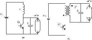
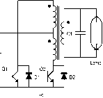 FIGURE 21.10 Nonresonant electronic ballasts. 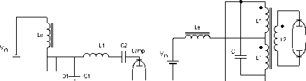 Lamp Lamp FIGURE 21.11 Three typical current-fed resonant inverters: (a) class E inverter, (b) current-fed push-pull inverter, and (c) current-fed full-bridge inverter. weight of the baUast. Fiowever, the adjustment of the circuit parameters to obtain optimum operation is quite difficult, especially for mass production. Another important drawback is the high voltage stress across the switch, which can reach values of three times the dc input voltage. For these reasons, the main applications of this circuit are battery supply baUasts with low input voltage and low lamp power, such as those used in emergency lighting and portable equipment. The typical power range of this baUast is 5 to 30 W. Applications of this circuit can be found in [18,19]. Another typical topology in this group is the current-fed push-puU inverter shown in Fig. 21.11b. In this circuit a dc input current is obtained by means of the choke inductor Le. Transistors are operated with a 50% duty cycle, thus providing a current square wave, which supplies the paraUel resonant circuit formed by the mutual inductance of the transformer and capacitor C. This circuit presents the advantage of being relatively easy to implement in a self-osciUating configuration, avoiding the use of extra control circuits and reducing cost. Also, zero-voltage switching (ZVS) can be obtained in the power switches. Fiowever, the switches also present a high voltage stress, about three times the dc input voltage, which make this topology unsuitable for power-hne applications. This circuit is also normally used in battery-operated applications in a self-oscillating arrangement. The typical power range is 4-100 W. Apphcations based on this circuit can be found in [20,21]. Finally, Fig. 21.11c shows a current-fed fuU-bridge resonant inverter, which can be used for higher power ratings. Also, this circuit aUows control of the output power at constant frequency by switching the devices of the same leg simultaneously, generating a quasi-square current wave through the resonant tank [6]. 21,2,2,2,2 Voltage-Fed Resonant Ballasts This type of baUast is one of those used most by electronic ballast manufacturers at the present time, especially for applications supplied from ac mains. The circuit is fed from a dc voltage source, normally obtained by line-voltage rectif)ing. A square-wave voltage waveform is then obtained by switching the transistors with a 50% duty cycle, and used to feed a series resonant circuit. This resonant tank filters the high-order harmonics and supplies the lamp with a sine current waveform. One advantage of the voltage-fed series resonant circuit is that starting voltage can be easily obtained without using extra ignition capacitors by operating close to the resonant tank frequency. Figure 21.12 shows electrical diagrams of typical voltage-fed resonant baUasts. The voltage-fed version of the push-puU inverter is iUustrated in Fig. 21.12a. This inverter includes a transformer, which can be used to step the input voltage up or down in order to obtain an adequate rms value of the output square wave voltage. This provides greater design flexibility but also increases cost. One disadvantage is that voltage across transistors is twice the input voltage, which can be quite high for line applications. Therefore, this inverter is normally used for low-voltage applications. Another important drawback of this voltage-fed inverter is that any asymmetry in the two primary windings (different number of turns) or in the switching times of power transistors would provide an undesirable dc level in the transformer magnetic flux, which in turn could saturate the core or decrease efficiency because of the circulation of dc currents. Figures 21.12b and 21.12c illustrates two possible arrangements for the voltage-fed half-bridge resonant inverter. The former is normally referred as the asymmetric half-bridge and uses one of the resonant tank capacitors (CI in the figure) to block the dc voltage level of the square wave generated by the bridge. This means that capacitor CI wiU exhibit a dc level equal to half the dc input voltage superimposed on its normal alternating voltage. A transformer can also be used in this inverter to step the input voltage up or down to the required level for each application. In this case the use of the series capacitor CI prevents any dc current from circulating through the primary winding, thus avoiding transformer saturation. This topology is often used by baUast manufacturers to supply fluorescent lamps, especially in the self-osciUating version, which aUows drastic reductions in cost. When supplying hot cathode fluorescent lamps, the paraUel capacitor C2 is normally placed across two electrodes, as shown in Fig. 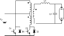 Lamp Lamp к 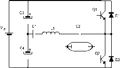 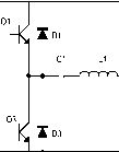 Lamp FIGURE 21.12 Typical voltage-fed resonant inverters: (a) push-pull; (b), (c) half bridge; and (d) full bridge. 21.12b, in order to provide a preheating current for the electrodes and achieve soft ignition. Figure 21.12c shows another version of the half-bridge topology, using two bulk capacitors to provide a floating voltage level equal to half the input voltage. In this case, capacitor Cl is no longer used to block a dc vohage, thus showing lower vohage stress. Finally, for the high power range (> 200 W), the fuU-bridge topology shown in Fig. 21.12d is normally used. Transistors of each half-bridge are operated with a 50% duty cycle and their switching signals are phase shifted by 180°. Thus, when switches Ql and Q2 are activated, direct voltage is applied to the resonant tank, and when switches Q3 and Q4 are activated the reverse voltage - is obtained across the resonant circuit. One of the advantages of this circuit is that the switching signals of the two branches can be phase shifted by angles between 0 and 180°, thus controlling the rms voltage apphed to the resonant tank in a range from 0 to У^ . This provides an additional parameter to control the output power at constant frequency, which is useful in implementing dimming ballasts. 21.3 Discharge Lamp Modeling The low frequency of the mains is not the most adequate power source for supplying discharge lamps. At these low frequencies electrons and ionized atoms have enough time to recombine at each current reversal. For this reason, the discharge must be reignited twice within each hne period. Figure 21.13a illustrates the current and voltage waveforms and the /-У characteristic of a 150-W HPS lamp operated with an inductive ballast at 50 Hz. As can be seen, the reignition voltage spike is nearly 50% higher than the normal discharge voltage, which is constant during the rest of the half-cycle. When lamps are operated at higher frequencies (above 5 kHz), electrons and ions do not have enough time to recombine. Therefore, charge carrier density is sufficiently high at each current reversal and no extra power is needed to reignite the lamp. The result is an increase in the luminous flux compared to that at low frequencies, which is especially high for fluorescent lamps (10-15%). Figure 21.13b shows the lamp waveforms and /-У characteristic for the same 150-W HPS when supplied at 50 kHz. The reignition voltage spikes disappear and the lamp behavior is nearly resistive. Figure 21.14 iUustrates how the voltage waveforms change in a fluorescent lamp when increasing the supply frequency. As can be seen, at a frequency of IkHz the voltage is already nearly sinusoidal and the lamp exhibits a resistive behavior. Therefore, a resistor can be used to model the lamp at high frequencies for baUast design purposes. However, most lamp manufacturers provide lamp data only for operation at low frequencies, where the lamp behaves as a square-wave voltage source. Table 21.2 shows the low-frequency electric data for different discharge lamps provided by the manufacturer and the measured values at high frequency for the same lamps. As 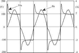 200 (V) 100 -100 -200 lla (a) 2 0 0.01 0.02 0.03 0.04 0.05 -200 -100 0 100 200 t (s) Via (V)
(a) lla (a) 2 1.5 -2 -1.5 0 10 20 30 40 t(is ) -200 -100 0 100 200 via (V) FIGURE 21.13 Waveforms and 7-У characteristics of 150-W HPS lamp at (a) 50 Hz; and (b) 50 kHz. 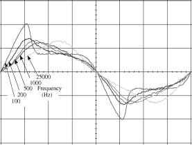 FIGURE 21.14 Voltage waveforms for a 36-W linear fluorescent lamp supplied through a resistive ballast at nominal power and different operating frequencies. Vertical scale: lOOV/div. can be seen, a power factor close to unity is obtained at high frequency. The equivalent lamp resistance at high frequencies can be easily estimated from the low-frequency data. Lamp power at any operating frequency can be expressed as foUows: Pla - УьАклРРьА (21.2) where V and 4л the rms values of lamp voltage and current, and FP is the lamp power factor. At hne frequencies the lamp power factor is low (typically 0.8) because of the high distortion in the lamp voltage waveform. FLowever, at high frequencies the lamp power factor reaches nearly 1.0. Then, lamp voltage and current at high frequency (У^д;,, I equation: la,hf) t)e estimated from the following la (21.3) hA,hfyLA,hf - ) TABLE 21.2 Electric data for different discharge lamps Manufacturer at 50 Hz Measured at High Frequency
Lamps aged for 100 hours. where Рц is the nominal lamp power provided by the manufacturer. As can be seen in Table 21.2, fluorescent lamps tend to maintain nearly the same rms current at low and high frequency, whereas high-pressure discharge lamps tends to maintain nearly the same rms voltage. Based on these assumptions, the equivalent lamp resistance at high frequency estimated from the low-frequency values is shown in Table 21.3. Low-pressure sodium lamps seem not to maintain either constant voltage or constant current at high frequency, and they also exhibit an equivalent resistance that is quite dependent on the frequency. Therefore, their equivalent resistance can only be obtained by laboratory testing. Note that the values given in Table 21.3 are only approximations of the real values, which should be obtained by measurement at the laboratory. They can be used as a starting point for the design of the electronic baUast, but final adjustments should be made in the laboratory. Another important issue is that lamp equivalent resistance is strongly dependent on power delivered to the lamp, which is especially important for designing electronic baUasts with dimming features. The characteristic lamp resistance versus lamp power is different for each discharge lamp type and must be obtained by laboratory testing. One of the best possibUities for fitting the lamp resistance versus power characteristic is the hyperbolic approximation. For example, Mader and Horn propose in [8] the following simple approximation: each lamp. This characteristic has been plotted in Fig. 21.15 for a particular lamp with Vq = 100 V and Pq = IW. This model can be implemented very easily in circuit simulation programs, such as SPICE-based programs. Figure 21.16 shows the electric circuit and the description used to model the lamp behavior in a SPICE-based simulation program. The voltage-controUed voltage source EL is used to model the resistive behavior of the lamp. The voltage source VS is used to measure the lamp current so that the instantaneous and average lamp power can be calculated; for this reason its voltage value is equal to zero. CP is a voltage-controUed power source used to calculate the instantaneous lamp power, which is then filtered by RP and CP in order to obtain the averaged lamp power. Finally, the hyperbolic relationship between lamp resistance and power is implemented by means of the voltage-controUed voltage source EK. The time constant т = RP CP is related to the ionization constant of the discharge. Figure 21.17 illustrates some simulation results at low frequency when the lamp is supplied from a sinusoidal voltage source and stabilized with an inductive baUast. The Mader-Horn model can also be used at high frequencies to give a resistive behavior for the lamp. The equivalent lamp resistance at high frequency wiU also exhibit a hyperbolic variation with the averaged lamp power and with a time constant given by т. This model is then useful to simulate electronic baUasts with dimming features. Rla(Pla) - PlaPo (21.4) where R is the equivalent lamp resistance, Рц is the average lamp power, and Vq two parameters that depend on TABLE 21.3 frequency Estimated electric data for discharge lamps at high
lOOOOr 5000 2500
0 5 10 15 20 Pla(W) FIGURE 21.15 Lamp resistance versus lamp power characteristic. 15 VS О О 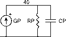 .subckt lamp 10 20 + params: V =100 P =1 Tau=0.3m E 10 15 Value={V(30,20)*I(VS)} VS 15 20 0 EK 30 20 Value={V *V /(V(40,20)+P )} К 30 20 1 GP 20 40 Value={V(10,20)*I(VS)} P 40 20 1 P 40 20 {Tau} . ends (a) (b) FIGURE 21.16 (a) Mader-Horn linear model for discharge lamps; and (b) SPICE description of the model. Vg Ы) 1 - 2Y;v LAMP I Vo=100V I Po=1W X=0.3ms Vg 1 0 SIN(0 325 50) b 1 2a 100 b 2a 2 500mH X A 2 0 AMP .tran 0.1m 60m 0 0.1m 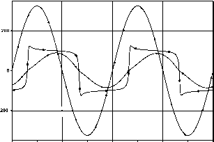 20ms 25ms 30ms 35ms 40ms 45ms 50ms 55ms 60ms ov(2) К1ЬГ50 *v(1) Time 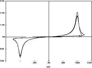 -150V -100V □ i(lb) (b) (c) FIGURE 21.17 (a) Example of simulation with an inductive ballast at low frequency; (b) Operating waveforms; and (c) Lamp 7-V characteristic. Discharge lamp modeling has become an important subject, because it is very useful in optimizing the electronic ballast performance. Some improvements on the Mader-FLorn model and other interesting models can be found in the literature [8-10]. 21.4 Resonant Inverters for Electronic Ballasts Most modern domestic and industrial electronic ballasts use resonant inverters to supply discharge lamps. They can be implemented in two basic ways: current-fed resonant inverters and voltage-fed resonant inverters. 21.4.1 Current-Fed Resonant Inverters One of the most popular topologies belonging to this category is the current-fed push-puU resonant inverter, previously shown in Fig. 21.11. For this reason, this inverter wiU be studied here to illustrate the operation of current-fed resonant ballasts. The current-fed push-puU inverter uses an input choke to obtain a dc input current with low current ripple. This current is alternately conducted by the switches so that a paraUel L < С 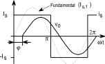 where is the base impedance of the resonant tank, Q is the normahzed load, Q is the normalized frequency, and cDq is the natural frequency of the resonant circuit, given by: = /l/C, Q = R/Zq, Q = ш/шо = ша/lC, Шо = l/VIC (21.8) FIGURE 21.18 (a) Equivalent circuit of a parallel resonant inverter; and (b) Operating waveforms. resonant tank can be supplied with a current square wave. Figure 21.18 shows the equivalent circuit and the operating waveforms of a current-fed resonant inverter. The input current can be expressed as a Fourier series in the following way: U0= E 4 sinna;/:= J2 -sinncot (21.5) =1.3.5... n=l,3,5... nn /5 is the peak value of each current harmonic, and /5 is the dc input current of the inverter. The output voltage for each current harmonic is obtained by multiplying the input current /5 by the equivalent parallel impedance : Уо,п - h,ne,n - h,n 1/R + jncoC - jil/ncDl) (21.6) Usually, normahzed values are employed in order to provide more general results. Then, the output voltage can be expressed as follows: l/Q + ;nQ-;(l/nQ) (21.7) From (21.7) the peak output voltage and phase angle cp can be obtained for each harmonic: Уо,п - h,nl (21.9) yi/Q2 + (nQ-l/nQ) cp = -tan Q(nQ - 1/nQ) (21.10) The total harmonic distortion (THD) of the output voltage can be calculated as foUows: o,n , я=3,5,7... THD(%) = ----100 (21.11) Based on these equations, the analysis and design of the current-fed resonant inverter can be performed. Normally, the circuit operates close to the natural frequency cOq, and the effect of the high-frequency harmonics can be neglected. To probe this. Fig. 21.19a illustrates the THD of the output voltage as a function of the normalized load and frequency, obtained by plotting (21.11). As can be seen, for values of Q greater than 1 and for operation close to the natural frequency (Q = 1), the THD is low, which means that the output voltage is nearly a sinusoidal waveform. However, for low values of Q the output voltage tends to be a square waveform, and the THD tends to a value of about 48%, corresponding to the THD of a square waveform. Figure 21.19b illustrates the normalized output voltage for the fundamental component. THD(%) 40
0.6 0.8 1 1.2 1.4 1.6 1.8 2 V0,1
0.4 0.6 0.8 1 1.2 1.4 1.6 1.8 2 FIGURE 21.19 Characteristics of the parallel resonant inverter: (a) THD; and (b) fundamental output voltage. As stated previously, when used as a lamp baUast the paraUel resonant inverter operates at the natural frequency of the resonant tank to both ignite the lamp and limit the current in normal operation. If we neglect the effect of high-order harmonics, the rms output voltage is given by the fundamental component and can be obtained using Q = 1 in (21.9) as foUows: Уо(гт$) УоМгтз) - 4,l(rms)sQ - 4IsR (21.12) In a current-fed resonant inverter, the dc input current Ig is supphed from a dc voltage source with a series choke, as stated previously. Then, the dc input current can be obtained, assuming 100% efficiency, by equaling input and output power as follows: o{rms) and then: Vl . o{rms) (21.13) (21.14) Using (21.14) in (21.12) and solving for the output voltage: (21.15) As can be seen, in operation at the natural frequency, the rms output voltage is independent of the resonant tank load. The peak output voltage is equal to nVJl. This value is directly related to the peak voltage stress in the switches. For a fuU bridge topology such as that shown in Fig. 21.11c, this value is equal to the switch voltage stress. Fiowever, for the current-fed push-puU inverter the voltage stress is twice this value, that is, яУ^ , because of the presence of the transformer. This gives a very high voltage stress for the switches in this topology, which is why the current-fed push-puU is mainly used to implement low-input-voltage baUasts. On the other hand, the lamp starting voltage can vary from 5 to 10 times the lamp voltage in normal discharge mode. This makes it difficult to use the paraUel resonant inverter at constant frequency to both ignite the lamp and supply it at steady state, since the output voltage is independent of the resonant tank load. One solution to this problem is to ignite the lamp at the resonant tank natural frequency and then change the frequency to decrease the output voltage and output current to the normal running values of the lamp. This solution makes necessary the use of extra circuitry to control the frequency, normally in a closed loop to avoid lamp instabUities, which increase baUast cost. Another solution, often used in low-cost baUasts, is to design the parallel resonant tank to ignite the lamp, and limit the lamp current in discharge mode by using an additional reactive element in series with the lamp. Normally a capacitor is used to limit the lamp current in order to minimize the cost of the ballast. This solution is used in combination with the self-osciUating technique, which ensures operation at a constant frequency equal to the natural frequency of the resonant tank. Figure 21.20a iUustrates this circuit. Normally the effect of the series capacitor is neglected and the resonant tank is assumed to behave as a sinusoidal voltage source during both ignition and normal operation, as shown in Fig. 21.20b. The high lamp starting voltage is obtained by means of a step-up transformer, which is why typically a push-puU topology is used. If is the dc input voltage and V is the lamp ignition voltage, then the necessary transformer turn ratio is given by the foUowing expression: 1 Угп1 (21.16) and the rms lamp current in discharge mode can be approximated as foUows: l.l(iV,/iVi)y, R + (l/2/Q) (21.17) R is the equivalent resistance of the lamp. From (21.17) the necessary value of the series capacitor Q used to limit the lamp current to the nominal value 4л be easily obtained. Finally, Figs. 21.21a and 21.21b illustrate a typical ballast based on a current-fed resonant inverter and its equivalent circuit, respectively. 21.4.2 Voltage-Fed Resonant Inverters Some voltage-fed resonant inverters used to supply discharge lamps were previously shown in Fig. 21.12. Basically, they use two or more switches to generate a square voltage waveform. The different topologies are mainly given by the type of resonant tank used to filter this voltage waveform. There are three typical resonant tanks, whose equivalent circuits are 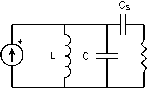 1-1Vin@ (a) FIGURE 21.20 (a) Typical parallel resonant circuit used to supply discharge lamps; and (b) Equivalent circuit. N1 Lm N1 Lm Lamp is® Le =---I. in Ш С (a) (b) FIGURE 21.21 (a) Self-oscillating current-fed push-pull electronic ballast, (b) Equivalent circuit. shown in Fig. 21.22. These circuits are the series-loaded resonant tank (Fig. 21.22a), the parallel-loaded resonant tank (Fig. 21.22b), and the series-parallel-loaded resonant tank (Fig. 21.22c). The typical operating waveforms are shown in Fig. 21.22d. Similarly to the current-fed resonant inverter, the input voltage can be expressed as a Fourier series in the foUowing way: 5(0= E VssmncDt= E --sinncDt (21.18) я=1,3,5... я=1,3,5... 71 v5 is the peak value of each voltage harmonic, and v5 the dc input voltage of the inverter. The same methodology used to analyze the current-fed resonant inverter wiU be used here to study the behavior of the three basic voltage-fed resonant inverters. 21.4.2.1 Series-Loaded Resonant Circuit The output voltage corresponding to the /7-order harmonic is easily obtained as foUows: (21.19) where Q5 and Q are the normalized load and switching frequency given by the foUowing expressions: = r/Zb = i(L/Q) / Q = ш/ш, = coyiQ (21.20) Figure 21.23a shows the THD of the series-loaded circuit and Fig. 21.23b shows the fundamental output voltage, which is normally considered for design purposes. In this circuit the input and output current are equal and can be calculated by dividing the output voltage by the load impedance. This current is also circulating through the inverter switches and therefore represents an important parameter for the design. Another important parameter is the phase angle of the input current, which defines the type of commutations in the inverter switches. For the fundamental harmonic, the phase angle of the current circulating through the resonant tank can be calculated as follows: (p = - tan (21.21) At the natural frequency (cOq) the input voltage and current wiU be in phase, which means that no reactive energy is handled by the circuit and aU the input energy is transferred to the load at steady-state operation. For frequencies higher than cOq, the current is lagged and some reactive energy wiU be R > Vo Vs ПЛ Cp :vo sCh > Vo Fundamental (Vg- ) 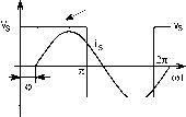 (a) (b) (c) (d) FIGURE 21.22 (a)-(c) Equivalent circuits of voltage-fed resonant inverters; and (d) typical operating waveforms. 1 ... 49 50 51 52 53 54 55 ... 91 |
|||||||||||||||||||||||||||||||||||||||||||||||||||||||||||||||||||||||||||||||||||||||||||||||||||||||||||||||||||||||||||||||||||||||||||||||||||||||||||||||||||||||||||||||||||||||||||||||||||||||||||||||||||||||||||||||||||||||||||||||||||||||||||||||||||||||||||||||||||||||||||||||||||||
|
© 2026 AutoElektrix.ru
Частичное копирование материалов разрешено при условии активной ссылки |