 |
 |
 |
| Главная Журналы Популярное Audi - почему их так назвали? Как появилась марка Bmw? Откуда появился Lexus? Достижения и устремления Mercedes-Benz Первые модели Chevrolet Электромобиль Nissan Leaf |
Главная » Журналы » Metal oxide semiconductor 1 ... 50 51 52 53 54 55 56 ... 91
Vo,l Vs,l 0.6 0.8 1 1.2 1.4 1.6 1.8
0.4 0.6 0.8 1 1.2 1.4 1.6 1.8 figure 21.23 Characteristics of series-loaded resonant inverter: (a) THD; and (b) fundamental output voltage. handled. In this case the inverter switches wiU present zero-voltage switching (ZVS) [22]. For frequencies lower than cOq, the current is in advance and also some reactive energy wiU be handled. In this case the inverter switches wiU present zero-current switching (ZCS). As can be seen in Fig. 21.23a, the TFiD is lower for the lower values of the normalized load and for frequencies close to the natural frequency of the resonant tank. For the higher values of Qs the TFiD tends to the value corresponding to a square wave. The output voltage is always lower than the input voltage, and for frequencies around the natural frequency the circuit behaves as a voltage source, especially for high values of Q. This means that the lamp cannot be ignited and supphed in discharge mode while maintaining constant switching frequency. This behavior is similar to that encountered for the current-fed resonant inverter. The use of step-up transformers is mandatory to achieve lamp ignition, especially for low input voltages. In order to maintain a constant operating frequency, a series element will be necessary to limit the lamp current at normal discharge operation. A capacitor can also be used, as discussed in a previous section. In summary, this circuit is mainly used in high-input-voltage, low-current apphcations, and it is not often used to implement electronic ballasts. 21.4.2.2 Parallel-Loaded Resonant Circuit In this circuit, the output voltage corresponding to the n-order harmonic is given by the following expression: V =Vc- o,n S,n (21.22) where: Qp = R/Zb = К(Ь/СрУ^\ Q = ш/шо = (о^/Щ (21.23) The TFiD and fundamental output voltage are shown in Fig. 21.24. This circuit presents characteristics that are much more useful in implementing electronic baUasts than the series-loaded resonant circuit. First, the TFiD of the output voltage around the natural frequency is in general much lower than that of the series circuit. For the lower values of Qp, the TFiD tends to a value of 12%, which corresponds to the TFiD of a triangular wave. As a result, the lamp voltage and current waveforms wiU be very simUar to a sine wave, which is the more adequate waveform to supply the lamp. Secondly, the frequency response of the output voltage (Fig. 21.24b) makes it possible to both ignite the lamp and limit the lamp current at steady state whUe maintaining constant operating frequency. During ignition the lamp behaves as a very high impedance, thus giving a high value of Qp. Under these conditions the paraUel circuit can generate a very high output voltage, provided that the operating frequency is close to the natural frequency. Once the lamp is ignited, the normahzed load Qp decreases and the circuit can limit the lamp current without changing the operating frequency. In fact, the paraUel circuit operating close to the natural frequency behaves as a current source for the load, as wiU be shown later. This behavior is very adequate to supply discharge lamps because it ensures good discharge stability, keeping the lamp from being easily extinguished by transitory power fluctuations. The maximum value of the voltage gain shown in Fig. 21.24 can be calculated to be equal to Qp/y/l - 1/4Q., and it appears at a frequency = 1 - l/2Qp. This means that a maximum is only present if Qp is greater than I/л/2 0.71. For the higher values of Qp, the maximum gain can be 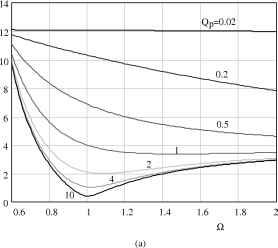 10 УоД Vs,l
0.4 0.6 0.8 1 1.2 1.4 1.6 1.8 figure 21.24 Characteristics of parallel-loaded resonant inverter: (a) THD; and (b) fundamental output voltage. approximated by Qp and the frequency of the maximum gain can be approximated to the natural frequency cOq. The input current of the paraUel resonant circuit is another important parameter to calculate the current handled by the inverter switches. Since the operating frequency is normally around resonance, only the fundamental component is considered. The value of this fundamental current and its phase angle can be obtained as foUows: 1 + QJQ (p = tan (21.24) (21.25) The condition for the input voltage being in phase with the input current can be obtained by equaling (21.25) to zero. This gives a value of the normalized frequency: Qq = yi - l/Ql. For a frequency greater than that value, the input current wiU lag the input voltage and the inverter switches wiU present zero-voltage switching. For frequencies lower than that value, the current wiU be in advance and zero-current switching is obtained. The output voltage gain at that frequency is equal to Qp. Finally, it is very interesting to study the behavior of this circuit for frequencies close to the natural frequency cDq (Q = 1), since this is the normal region selected to operate for baUast applications. At this frequency, the output voltage gain is equal to Qp and then the output current wiU be Vi/Zg. This means that when operated at the natural frequency the parallel circuit behaves as a current source, whose value depends only on the input voltage. At the natural frequency the input current is equal to Vy/l + Ql/Z and the phase angle is equal to tan~(-1/Qp). The behavior of the circuit is always inductive, with zero-voltage switching, and the phase angle decreases with increasing Qp, which means that less reactive energy is handled by the circuit. 21.4.2.3 Series-Parallel-Loaded Resonant Circuit This circuit is also often used to implement electronic baUasts. The fundamental output voltage is given by the foUowing expression: n,i = s,r (21.26) where: Qp = R/Zs = К(1/СеГ'\ Q = = (DLC~e, a = Ce/Cp = 1 - Ce/Cs (21.27) and Q = QCp/(Q + Cp) is the series equivalent of the two capacitors present in this resonant circuit. The fundamental input current and its phase angle are the foUowing: -l/2 (p = (21.28) - tan Qsp -1 + 180° , -a tan -- - tan QspQ. Qsp ii-i if Q < = Vl - a if Q > = Vl - a (21.29) Figure 21.25 shows the characteristics corresponding to the TFiD of the output voltage and the fundamental output voltage for a = 0.5. As can be seen, the TFiD is also very low around the natural frequency, especially for the higher values of the normalized load Qp. Regarding the output voltage, this circuit behaves as a parallel circuit around the natural frequency cOq, with a maximum gain voltage of about Qp/a. Around the natural frequency of the series circuit given by L and q, cOq = cOqVI - a? the circuit behaves as a series-loaded circuit with a maximum voltage gain equal to unity. The series-paraUel circuit can also be used to both ignite and supply the lamp at constant frequency, since it also behaves as a current source at the natural frequency. Besides, this circuit aUows limiting the ignition voltage by means of the factor a, thus avoiding sputtering damage of lamp electrodes. Also, the series capacitor can be used to block any dc component of the inverter square output voltage, such as that existing in the asymmetric half-bridge. In summary, the series-parallel circuit combines the best features of the series-loaded and the parallel-loaded circuits, and this is why it is often used to implement electronic ballasts. When operated at frequency cOq the output voltage gain is equal to Qp/a, and then the circuit behaves as a current source equal to Vj/aZg, which is independent of the load. As stated previously, this is very adequate for supplying discharge lamps. The input current phase angle at this frequency is equal to tan~(-a/Qp), and the input current always lags the input voltage, thus showing zero-voltage switching. Finally, the condition to have input current in phase with the input voltage can be obtained by setting (21.29) equal to zero. This gives the foUowing value: QsP,(p=0 - 7  (21.30) Equation (21.30) defines the borderline between zero-voltage switching and zero-current switching modes. The output voltage gain in this borderhne can be obtained by using (21.30) in (21.26), and it is equal to (х ф - Q). 21.4.3 Design Issues The design methodology of a resonant inverter for discharge-lamp supply can be very different depending on the lamp type and characteristics, inverter topology, design goals, etc. Some guidehnes focused especially on supplying fluorescent lamps with voltage-fed resonant inverters are presented in this section to illustrate the basic design methodology. A typical starting process for a hot cathode fluorescent lamp is shown in Fig. 21.26. Initially, lamp electrodes are heated up to the emission temperature. During this phase, the inverter should ensure a voltage applied to the lamp that is not high enough to produce sputtering damage in lamp electrodes, thus avoiding premature aging of the lamp. Once electrodes reach the emission temperature, the lamp can be ignited by applying the necessary starting voltage. FoUowing this procedure, soft starting is achieved and long lamp life is ensured. The best method to perform this soft starting is to control the inverter switching frequency so that the lamp voltage and current are always under control. During the heating process the operating frequency is adjusted to a value over the natural frequency of the resonant tank. In this way, the heating current can be adjusted to the necessary value, maintaining a lamp voltage that is much lower than the starting voltage. Since normally MOSFET or bipolar transistors are used, operation over the natural frequency is preferable, because it provides ZVS and the slow parasitic diodes existing in these transistors can be used. After a short period of time, the switching frequency is reduced until the starting voltage is obtained; then the lamp is ignited. Normally, the final operating point at
0.5 0.6 0.7 0.8 0.9 1 1.1 1.2 1.3 1.4 1.5 10 УоД Vs,l
0.5 0.6 0.7 0.8 0.9 1.1 1.2 1.3 figure 21.25 Characteristics of series-parallel-loaded resonant inverter: (a) THD; and (b) fundamental output voltage.
figure 21.26 Typical starting process of discharge lamps. Steady-State operation is adjusted to be at a switching frequency equal to the natural frequency, so that very stable operation for the lamp is ensured. Figure 21.27a shows a fluorescent lamp supplied using a series-parallel resonant tank. The input data for the design are normally the fundamental input voltage V, the switching frequency in normal discharge operation (running) /5, the lamp voltage and current at high frequency Yj, 4л, the electrode heating current 4, the maximum lamp voltage during heating process Vjj, and the lamp starting voltage Yiq. The equivalent circuit during the heating and ignition phase is shown in Fig. 1\21\. The current circulating in this circuit is the electrode heating current, which can be calculated by using = 00 in (21.28): Q- 1/Q (21.31) where the electrode resistance has been neglected for simphcity. For a given heating current l, the necessary switching frequency is obtained from (21.31) as follows: Regarding the heating voltage, it can be calculated from (21.26) using = 00, and the following value is obtained: (21.33) The frequency at which the starting voltage is achieved can also be obtained following value: using = 00 in (21.26), giving the (21.34) Once the lamp is ignited, the new operating circuit is shown in Fig. 21.27c. Normally the switching frequency is selected to be very close to the natural frequency, and the circuit characteristics can be obtained by setting Q = 1. Thus, as stated previously, the circuit behaves as a current source of the following value: Ila = (21.35) From this equation the impedance needed to provide a lamp current equal to is easily obtained: (21.36) Using Eqs. (21.31)-(21.36), the design procedure can be performed as follows: Step 1: Steady-state operation. Choose a value for the factor a; normally a value of 0.8-0.9 will be adequate for most applications. From (21.36) calculate the value of for the resonant tank. Since the natural frequency is equal to the switching frequency, the reactive elements of the resonant tank can be calculated as follows: 2ZbI (21.32) 2nfs 2nfsCcZB 271/5(1 - a)Zs (21.37)  Vh V3 0 Rla> Cp: figure 21.27 (a) Fluorescent lamp supplied with a series-parallel circuit; (b) equivalent circuit during heating and ignition; and (c) equivalent circuit during normal discharge mode. Step 2: Heating phase. From (21.32) calculate the switching frequency for a given heating current 1. Then, calculate the value of the heating voltage from (21.33). Step 3: Check if the heating voltage is lower than the maximum value allowed to avoid electrode sputtering. If the voltage is too high, choose a lower value of a and repeat steps 1 and 2. Also, the maximum heating frequency can be limited to avoid excessive frequency variation. The lower the value of a, the lower the frequency variation from heating to ignition, since the output voltage characteristics are narrower for the lower values of a. The described procedure to achieve lamp soft ignition requires the use of a voltage-controUed osciUator to control the switching frequency. This can increase the cost of the ballast. A simUar soft ignition can be achieved using the resonant circuit shown in Fig. 21.28. This circuit is often used in self-oscillating baUasts, where the switches are driven from the resonant current using a current transformer [23]. In the circuit shown in Fig. 21.28, the PTC is initially cold and capacitor Cpi is bypassed by the PTC. The resonant tank under these conditions is formed by L-Cg-Cp2, which can be designed to heat the lamp electrodes with a heating voltage low enough to avoid lamp cold ignition. Since the PTC is also heated by the circulating current, after a certain period of time it reaches the threshold temperature and trips. At this moment, the new resonant tank is formed by I, Q, and the series equivalent of Cp and Cp2. This circuit can be designed to generate the necessary ignition voltage and to supply the lamp in normal discharge mode. Once the lamp is ignited, the PTC maintains its high impedance since the dominant paraUel capacitor in this phase is Cp (usually Cp < Срз). 21.5 High-Power-Factor Electronic Ballasts As mentioned in a previous section, when electronic baUasts are supphed from the ac line an ac-dc stage is necessary to provide the dc input voltage of the resonant inverter (see Fig. 21.9). Since the introduction of harmonic regulations, such as lEC 1000-3-2, the use of a fuU-bridge diode rectifier followed by a filter capacitor is no longer applicable for this stage because of the high harmonic content of the input current. Therefore, the use of an ac-dc stage showing a high input power factor (PF) and a low total harmonic distortion (TFiD) of the input current is mandatory. The inclusion of this stage can greatly increase the cost of the complete ballast, and therefore the search for low-cost, high-power-factor electronic baUasts is an important field of research at present. Figure 21.29a shows a first possibility to increase the input power factor of the baUast by removing the filter capacitor across the diode rectifier. Fiowever, since there are no low-frequency storage elements inside the resonant inverter, the output power instantaneously foUows the input power, thus producing an annoying hght flicker. Besides, the resulting lamp current crest factor is very high, which considerably decreases lamp life. In order to avoid flicker and increase lamp current crest factor, continuous power must be delivered to the lamp. This can only be accomplished by using a PFC stage with a low-frequency storage element. This solution is shown in Fig. 21.29b, where capacitor Q is used as energy storage element. The main drawback of this solution is that the input power is handled by the two stages, which reduces the efficiency of the complete electronic baUast. Lamp Cpi: CP2- FIGURE 21.28 Resonant circuit using a PTC resistor. 21.5.1 Harmonic Limiting Standards The standards lEC 1000-3-2 and EN 61000-3-2 [24] are the most popular regulations regarding the harmonic poUution produced by electronic equipment connected to mains. These standards are a new version of the previous lEC 555-2 regulation and they are applicable to equipment with less than 16 A per phase and supplied from low-voltage lines of 220/380 V, 230/400 V, and 240/415 V at 50 or 60 Hz. Limits RESONANT INVERTER lamp
FIGURE 21.29 High-power-factor ballasts. RESONANT INVERTER lamp TABLE 21.4 lEC 1000-3-2: harmonic Hmits for class С equipment Harmonic order n 2 3 5 7 9 11 <л <39 (odd harmonics only) Maximum Permissible Harmonic Current Expressed as a Percentage of the Input Current at the Fundamental Frequency 30Г 10 Я is the circuit power factor for equipment supplied from voltages lower than 220 V have not yet been established. This regulation divides electric equipment into several classes from class A to class D. Class С is especially for lighting equipment, including dimming devices; the harmonic hmits for this class are shown in Table 21.4. As shown in the table, this regulation establishes a maximum amplitude for each input harmonic as a percentage of the fundamental harmonic component. The harmonic content established in Table 21.4 is quite restrictive, which means that the input current wave must be quite similar to a pure sine wave. For example, for a typical input power factor equal to 0.9 the total harmonic distortion calculated from Table 21.1 is only 32%. 21.5.2 Passive Solutions A first possibility to increase the ballast power factor and to decrease the harmonic content of the input current is the use of passive solutions. Figure 21.30 shows two typical passive solutions, which can be used to improve the input power factor of electronic baUasts. Figure 21.30a shows the most common passive solution based on a filter inductor L Using a large inductance L a square input current can be obtained, with an input power factor of 0.9 and a THD of about 48%. A square input waveform does not satisfy the lEC 1000-3-2 requirements and thus is not a suitable solution. The addition of capacitor С across the ac terminals can increase the power factor to 0.95, but StiU the standard requirements are difficult to fulfiU. Co = Co = (a) (b) FIGURE 21.30 Passive circuits to improve input power factor: (a) LC filter; and (b) tuned LC filter. A simple variation of this circuit is shown in Fig. 21.30b, where a parallel circuit tuned to the third harmonic of the line frequency is used to improve the shape of the line current. The input power factor obtained with this circuit can be close to unity. A third possible solution, known as the vaUey-fiU circuit, is shown in Fig. 21.31a. The typical filter capacitor following the diode rectifier is split into two different capacitors that are alternately charged using three extra diodes. The addition of a smaU series resistor improves the power factor in about two points, maintaining low cost for the circuit. An inductor in place of the resistor can also be used to improve the power factor, but with a higher cost penalty. Figure 21.31b shows the output voltage and input current of the vaUey-fiU circuit. The main disadvantage of this circuit is the high ripple of the output voltage, which produces lamp power and luminous flux fluctuation and high lamp current crest factor. Passive solutions are reliable, rugged, and cheap. However, the size and weight of these solutions are high and their design to fulfiU the lEC 1000-3-2 requirements is usually difficuh. Therefore, they are normally applied in the lower power range. 21.5.3 Active Solutions Active circuits are the most popular solutions for implementing high-power-factor electronic ballasts. They use controUed switches to correct the input power factor and in some cases to include galvanic isolation via high-frequency transformers. Active circuits normally used in electronic baUasts operate at a switching frequency weU above the line frequency and over the audible range. Some typical active circuits used in electronic baUasts are shown in Fig. 21.32. Buck-boost and flyback converters, shown in Figs. 21.32a and 21.32b, respectively, can be operated in discontinuous conduction mode (DCM) with constant frequency and constant duty cycle in order to obtain an input power factor close to unity [25]. Figure 21.32c shows the boost converter, which is one of the most popular active circuits used to correct the input power factor of electronic ballasts [26-28]. If the boost converter is operated in DCM, an input power factor close to unity is obtained, provided that the output voltage is about twice the peak input voltage [26]. The main disadvantage of DCM operation, when compared to the CCM mode, is the high distortion of the input current (due to the discontinuous high-frequency current) and the higher current and voltage stresses in the switches. Therefore, DCM operation is only used for the lower power range. For the medium power range, the operation of the boost converter at the DCM-CCM borderline is preferred. In this solution the on time of the controUed switch is maintained constant within the whole line period, and the switching frequency is adjusted to aUow the input current to reach zero at the end of the switching period. The typical control 400V  -200V
1.0A -0.5A - -0.5A 450ms 460ms 470ms 480ms Time 490ms 500ms (a) (b) FIGURE 21.31 Valley-fill circuit: (a) circuit diagram; and (b) waveforms. 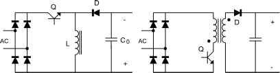 Co AC (a) (b) (c) FIGURE 21.32 Power factor correction circuits for ballasts: (a) buck-boost; (b) flyback; and (c) boost. circuit used and the input current waveform are shown in Figs. 21.33a and 21.33b, respectively. The inductor current is sensed using a resistor in series with the switch, and the peak inductor current is programmed to foUow a sine wave using a multiplier. A comparator is employed to detect the zero-crossing of the inductor current in order to activate the switch. Most 1С manufacturers provide a commercial version of this circuit to be used for electronic ballast apphcations. The boost circuit operating with borderhne control provides a continuous input current, which is easier to filter. It also presents low switch turn-on losses and low recovery losses in the output diode. The main disadvantages are the variable switching frequency and the high output voltage, which must be higher than the peak line voltage. For the higher power range, the boost converter can be operated in continuous conduction mode (CCM) to correct the input power factor. The input current in this scheme is continuous with very low distortion and easy to filter. The current stress in the switch is also lower, which means that more power can be handled, maintaining good efficiency. The normal efficiency obtained with a boost circuit operating either in the DCM-CCM borderhne or in CCM can be as high as 95%. 21.6 Applications Electronic ballasts are widely used in lighting applications such as portable lighting, emergency lighting, automotive applications, home lighting, and industrial lighting. They provide low volume and size, making it possible to reduce the luminaire size as weU, with very interesting results for the new trends in lighting design. 21.6.1 Portable Lighting In this apphcation a battery is used as power source and then a low input voltage is available to supply the lamp. Examples are hand lanterns and back-lighting for laptop computers. Typical input voltages in these applications range from 1.5 to 48 V. Therefore, a step-up converter is necessary to supply the discharge lamp, and then electronic baUasts are the only 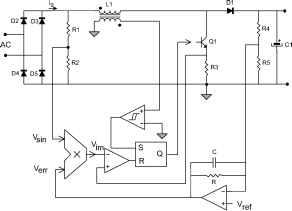 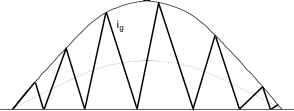 Q1 CONTROL SIGNAL FIGURE 21.33 (a) Boost power factor corrector with borderUne control; and (b) input current waveform. suitable solution. Since the converter is supplied from a battery, the efficiency of the ballast should be as high as possible in order to optimize the use of the battery energy, thus increasing the operation time of the portable lighting. Typical topologies used are the class E inverter and the push-puU resonant inverter, providing efficiencies up to 95%. 21.6.2 Emergency Lighting Emergency lighting is used to provide a minimum lighting level in case of a main supply cutoff. Batteries are employed to store energy from the mains and to supply the lamp in case of a main supply failure. A typical block diagram is shown in Fig. 21.34. An ac-dc converter is used as battery charger to store energy during normal line operation. A control circuit continuously measures the line voltage and activates the inverter in case of a main supply failure. Normally a minimum operating time of 1 hour is required for the system in emergency state; thus the use of high-efficiency electronic ballasts is mandatory to reduce battery size and cost. Typical topologies used include class E inverters, push-pull resonant inverters, and half-bridge resonant inverters. Fluorescent lamps are mainly used in emergency ballasts, but high-
LAMP \f CONTROL CIRCUIT FIGURE 21.34 Block diagram of an emergency lighting system. intensity discharge lamps, such as metal hahde lamps or high-pressure sodium lamps, are also used in some special applications. 21.6.3 Automotive Lighting Electronic ballasts are used in automotive apphcations such as automobiles, buses, trains, and aircraft. Normally a low-voltage dc bus is available to supply the lamps, and then these apphcations are similar to the portable and emergency hghting previously discussed. In modern aircraft a 120/208 V, 400 Hz, three-phase electrical system is also available and can be employed for lighting. Fluorescent lamps are typically used for automotive indoor lighting, whereas high-intensity discharge lamps are preferred in exterior lighting, for example, in automobile headlights. 21.6.4 Home and Industrial Lighting Electronic ballasts, especially for fluorescent lamps, are also often used in home and industrial apphcations. The higher efficiency of fluorescent lamps supplied at high frequency provides significant energy savings when compared to incandescent lamps. A typical application is the use of compact fluorescent lamps with the electronic ballast inside the lamp base, which can directly substitute for an incandescent lamp, reducing the energy consumption by a factor of 4 or 5. A self-oscillating half-bridge inverter is typically used in these energy-saving lamps, since it aUows reduced size and cost. The power of these lamps is normally below 25 W. Other applications for higher power include more developed baUasts based on a power factor correction stage foUowed by a resonant inverter. Hot cathode fluorescent lamps are the most used in these electronic baUasts. Also, with the development of modern HID lamps such as metal halide lamps and very high pressure sodium lamps (both showing very good lamp1  lamp2 power line communication stage microprocessor control stage FIGURE 21.35 Block diagram of microprocessor-based lighting. color rendition), the use of FilD lamps is becoming more frequent in home, commercial, and industrial lighting. 21.6.5 Microprocessor-Based Lighting The use of microprocessors in combination with electronic ballasts is very interesting from the point of view of energy savings [29-31]. The inclusion of microprocessor circuits allows incorporation of control strategies for dimming such as scheduling, task tuning, and daylighting [2]. Using these strategies, the energy savings achieved can be as great as 35-40%. Another advantage of using microprocessors is the possibility of detecting lamp failure or bad operation, thus increasing reliability and decreasing the maintenance cost of the installation. Most advanced electronic baUasts can include a communication stage to send and receive information regarding the state of the lighting to or from a central control unit. In some cases communications can be performed via power line, thus reducing installation costs. Figure 21.35 shows the block diagram of a microprocessor-based electronic ballast. References Books 1. Illuminating Engineering Society of North America: IBS Lighting Handbook 1984 Reference Volume, lESNA, New York, 1984. 2. Illuminating Engineering Society of North America: lES Lighting Handbook 1984 Application Volume, lESNA, New York, 1987. 3. Meyer, Chr., and Nienhuis, H.: Discharge Lamps, Philips Technical Library, 1988. 4. De Groot, J., and Van Vliet, J.: The High-Pressure Sodium Lamp. Philips Technical Library, Macmillan Education, 1986. 5. Wyszecki, G., and Stiles, W. S.: Color Science: Concepts and Methods, Quantitative Data and Formulae, 2nd edition. John Wiley & Sons, 1982. 6. M. H. Rashid: Power Electronics. Circuits, Devices, and Applications, 2nd edition. Prentice Hall. New Jersey, 1993. Articles 7. Borton, J. A., and Daley, K. A.: A comparison of light sources for the petrochemical industry, IEEE Industry Applications Magazine, pp. 54-62, July/August 1997. 8. Mader, U., and Horn, P.: A dynamic model for the electrical characteristics of fluorescent lamps, IEEE Industry Applications Society Meeting, Conf Records, pp. 1928-1934, 1992. 9. Sun, M., and Hesterman, B. L.: Pspice high-frequency dynamic fluorescent lamp model, IEEE Trans, on Power Electronics, Vol. 13, No. 2, pp. 261-272, March 1998. 10. Tseng, K.-J., Wang, Y, and Vilathgamuwa: An experimentally verified hybrid Cassie-Mayr electric arc model for power electronics simulations, IEEE Trans, on Power Electronics, Vol. 12, No. 3, pp. 429- 436, May 1997. 11. Ailing, W R.: Important design parameters for solid-state ballasts, IEEE Transactions on Industry Applications, Vol. 25, No. 2, pp. 203-207, March/April 1989. 12. Koshimura, Y, Aoike, N., and Nomura, O.: Stable high frequency operation of high intensity discharge lamps and their ballast design, Proc. CIE 20th Session 83, pp. E36/1-E36/2, 1983. 13. Laskai, L., Enjeti, P. N., and Pitel, 1. J.: White-noise modulation of high-frequency high-intensity discharge lamp ballasts, IEEE Transactions on Industry Applications, Vol. 34, No. 3, pp. 597-605, May/June 1998. 14. Simoes, A. S., Silva, M. M., and Anunciada, A. V: A boost-type converter for DC-supply of fluorescent lamps, IEEE Transactions on Industrial Electronics, Vol. 41, No. 2, pp. 251-255, April 1994. 15. Vasiljevic, D. M.: The design of a battery-operated fluorescent lamp, IEEE Transactions on Industrial Electronics, Vol. 36, No. 4, pp. 499-503, November 1989. 16. Hernando, M., Blanco, C, Alonso, J. M., and Rico, M.: Fluorescent lamps supplied with dc current and controlled in current mode, Proc. European Power Electronics Conference (EPE), pp. 1/499-1/503, Firenze, 1991. 17. Corominas, E. L., Alonso, J. M., Calleja, A. J., Ribas, J., and Rico, M.: Analysis of tapped-inductor inverters as low-power fluorescent lamp ballast supplied from a very low input voltage, PESC Conf Record, pp. 1103-1108, 1999. 18. Duarte, J. L., Wijntjens, J., and Rozenboom, J.: Getting more from fluorescent lamps through resonant converters, Proc. lECON, San Diego, pp. 560-563, 1992. 19. Ponce, M., Aran, J., Alonso, J. M., and Rico-Secades, M.: Electronic ballast based on class E amplifier with a capacitive inverter and dimming for photovoltaic applications, Proc. APEC, pp. 1156-1162, 1998. 20. Gulko, M., and Ben-Yaakov, S.: Current-sourcing push-pull parallel-resonance inverter (CS-PPRI): theory and application as a discharge lamp driver, IEEE Transactions on Industrial Electronics, Vol. 41, No. 3, pp. 285-291, June 1994. 21. Lin, M.-S., Ho, W-J., Shih, R-Y, Chen, D.-Y, and Wu, Y-R: A cold-cathode fluorescent lamp driver circuit with synchronous primary-side dimming control, IEEE Transactions on Industrial Electronics, Vol. 45, No. 2, pp. 249-255, April 1998. 22. Alonso, J. M., Blanco, C, Lopez, E., Calleja, A. J. and Rico, M.: Analysis, design and optimization of the LCC resonant inverter as a high-intensity discharge lamp ballast, IEEE Trans, on Power Electronics, Vol. 13, No. 3, pp. 573-585, May 1998. 23. Electronics ballasts for fluorescent lamps using BUL770/791 transistors. Application Report, Texas Instruments, 1992. 24. lEC 1000-3-2 (1995-03) standards on electromagnetic compatibility (EMC), Part 3, Section 2: Limits for harmonic current emissions. International Electrotechnical Commission, Geneva, Switzerland, April 1995. 25. Alonso, J. M., Calleja, A. J., Lopez, E., Ribas, J., and Rico, M.: A novel single-stage constant-wattage high-power-factor electronic ballast, IEEE Trans, on Industrial Electronics, Vol. 46, No. 6, pp. 1148-1158, December 1999. 26. Liu, K.-H., and Lin, Y.-L: Current waveform distortion in power factor correction circuits employing discontinuous-mode boost converters, Power Electronics SpeciaHsts Conference proceedings, pp. 825-829, 1989. 27. Lai, J. S., and Chen, D.: Design consideration for power factor correction boost converter operating at the boundary of continuous conduction mode and discontinuous conduction mode, AppHed Power Electronics Conference Proceedings, pp. 267-273, 1993. 28. Blanco, C, Alonso, J. M., Lopez, E., Calleja, A. J., and Rico, M.: A single-stage fluorescent lamp ballast with high power factor, IEEE APEC 96 Proceedings, pp. 616-621. 29. AlHng, W. R.: The integration of microcomputers and controllable output baUasts - A new dimension in lighting control, IEEE Trans, on Industry Applications, pp. 1198-1205, September/October 1984. 30. Alonso, J. M., Diaz, J., Blanco, C, and Rico, M.: A microcontroller-based emergency ballast for fluorescent lamps, IEEE Transactions on Industrial Electronics, Vol. 44, No. 2, pp. 207-216, April 1997. 31. Alonso, J. M., Ribas, J., Calleja, A. J., Lopez, E., and Rico, M.: An intelligent neuron-chip-based fluorescent lamp ballast for indoor applications , Conf. Proc. of the IEEE Industry Applications Society Annual Meeting (IAS 97), pp. 2388-2394, New Orleans, Louisiana, October 5-9, 1997. 1 ... 50 51 52 53 54 55 56 ... 91 |
||||||||||||||||||||||||||||||||||||||||||||||||||||||||||||||||||||||||||||||||||||||||||||||||||||||||||||||||||||||||||||||||||||||||||||||||||||||||||||||||||||||||||||||||||||||||||||||||||||||||||||||||||||||||||||||||||||||||||||||||||||||||||||||||||||||||||||
|
© 2026 AutoElektrix.ru
Частичное копирование материалов разрешено при условии активной ссылки |