 |
 |
 |
| Главная Журналы Популярное Audi - почему их так назвали? Как появилась марка Bmw? Откуда появился Lexus? Достижения и устремления Mercedes-Benz Первые модели Chevrolet Электромобиль Nissan Leaf |
Главная » Журналы » Metal oxide semiconductor 1 ... 51 52 53 54 55 56 57 ... 91 Power Electronics in Capacitor Charging Applications R. Mark Nelms, Ph.D. Department of Electrical and Computer Engineering 200 Broun Hall Auburn University, Auburn Alabama 36849 22.1 Introduction...................................................................................... 533 22.2 High-Voltage dc Power Supply with Charging Resistor............................. 533 22.3 Resonance Charging............................................................................ 534 22.4 Switching Converters........................................................................... 535 References.......................................................................................... 537 22.1 Introduction Conventional dc power supplies are designed to operate at a given output voltage into a constant or near-constant load. Pulse lasers, flashlamps, railguns, and other pulse power systems, however, require short but intense bursts of energy that may be derived from rapidly charging an energy storage capacitor. The rate at which the capacitor is discharged is caUed the repetition rate and may vary from 0.01 Hz for large capacitor banks to a few kilohertz for certain lasers. After the energy storage capacitor is discharged, it must be recharged to a specified voltage using a capacitor charging power supply (CCPS). The utilization of power electronics in capacitor charging apphcations is presented in this chapter. Figure 22.1 shows the voltage across the energy storage capacitor connected to the output of a CCPS. As seen in this figure, the CCPS has three modes of operation. The first mode is the charging mode, in which the capacitor is charged from an initial voltage of zero to a specified final voltage. The duration of the charging mode is determined by the capacitance of the energy storage capacitor. The next mode of operation is the refresh mode, which can be considered a standby mode. When the output voltage drops below a predetermined value, the CCPS should turn on and deliver the energy necessary to compensate for capacitor leakage. The duration of the refresh mode is determined by the loads repetition rate (l/T). The final mode of operation is the discharge mode, where the load is discharging the capacitor. The CCPS does not supply any energy to the load in this mode. The amount of time the CCPS remains in this mode is determined by how quickly the load can discharge the capacitor. The instantaneous output power for a CCPS varies over a wide range in comparison to a conventional dc power supply, which supphes a constant or near-constant power to its load. This is shown in Fig. 22.2; the output power for the pulsed power load is drawn as linear for iUustration purposes only. The charging mode is characterized by high peak power. At the beginning of this mode, the output power is zero (i.e., there is no voltage present but current is flowing). Thus, the load capacitor is equivalent to a short circuit. Additionally, at the end of the charging mode, the output power is again zero (i.e., there is an output voltage present but no current is flowing). Now the load capacitor is equivalent to an open circuit. The refresh mode is typically a low-power mode, because the current required to compensate for capacitor leakage is smaU. The CCPS does not supply any power during the discharge mode when the energy storage capacitor is being discharged by the pulsed load. The average output power for a CCPS depends on the repetition rate of the load. It is a maximum when the energy storage capacitor is discharged at the end of the charging mode, which corresponds to operation without a refresh mode. Since the average output power is affected by the repetition rate of the load, the rating of a CCPS is often given in kj/s instead of kW. The kj/s rating indicates how fast a particular capacitor can be charged to a given voltage. 22.2 High-Voltage dc Power Supply with Charging Resistor In this technique, the energy storage capacitor is charged by a high-voltage dc power supply through a charging resistor as Refresh Mode 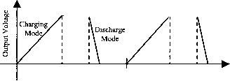 Repetition Rate = 1/T j FIGURE 22.1 Three modes of operation of a capacitor charging power supply. Pulsed Power Load Constant Power Load 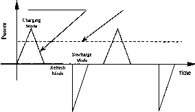 FIGURE 22.2 Power requirements for pulsed power and constant power loads.
FIGURE 22.3 High-voltage dc power supply and charging resistor. illustrated in Fig. 22.3. The charging mode ends when the capacitor voltage equals the output voltage of the power supply. The capacitor is continually refreshed by the power supply. During the discharge mode, the charging resistor isolates the power supply from the pulse load. The advantages of this technique are its simphcity, reliability, and low cost. The major disadvantage of this technique is its poor efficiency. In the charging mode, the energy dissipated in the charging resistor is equal to the energy stored in the capacitor in the ideal case; therefore, the maximum efficiency is 50%. As a result, this technique is utilized only in applications where the charge rate is low, i.e., 200 J/s. Another disadvantage of this technique is related to the charge time, which is determined by the RC time constant. Some laser applications require that the output voltage be within 0.1% of a target voltage. For this technique, more than five time constants are required for the capacitor voltage to meet this voltage specification. 22.3 Resonance Charging The basic resonance charging technique is illustrated in Fig. 22.4. An ac input voltage is stepped up with a transformer, rectified, and filtered with capacitor c2 to produce a high dc voltage Vq- this circuit, c2 is much greater than Q. Thyristor Tl is gated and current flows through the inductor and diode D, transferring energy from c2 to Q. The voltage v(t) and current i(t) are described by the foUowing equations assuming that c2 Q. The charge time, t, for this circuit can be calculated by finding the time at which the current described by Eq. (22.2) reaches zero and is given below. The voltage v(t) has a value of 2Vq at the end of the charging mode. v(t) = Vo(l -coscOoO Kt) = Voysincoot /LCi t, = n/ICi = - (22.1) (22.2) (22.3) (22.4) Even though this technique is simple and efficient, it is not without its limitations. A high-voltage capacitor with a large capacitance value is needed for c2, which increases the cost. A single thyristor is shown in Fig. 22.4. Multiple thyristors connected in series or a thyratron may be required, depending on the voltage level. The repetition rate of the pulse load should be such that Q is fully charged and i(t) has reached zero before the load discharges to prevent latch-up of T. It is not possible for this circuit to operate in the refresh mode because of the switch characteristics. Therefore, v(t) wiU drift as a result of capacitor leakage. The charge time is a function of the circuit parameters and wiU drift as they change with temperature or due to aging. Since aU of the energy stored in Q is transmitted from c2 in a single pulse, it can be difficult to achieve a very smaU voltage regulation with the resonance charging technique. However, regulation can be improved with the addition of a dequeing circuit as shown in Fig. 22.5. The voltage v(t) is monitored with a sensing network. Just before v(t) reaches the desired level, thyristor t2 is fired, which terminates the charging mode. The remaining energy stored in the inductor is dissipated in R. The addition of the dequeing circuit reduces circuit  i(t) v(t) Pulse Load FIGURE 22.4 Resonance charging.  Rectifier  [--1 Control I  Pulse Load figure 22.5 Resonance charging with dequeing. efficiency and increases the circuit complexity and cost, but does not enable a refresh mode to compensate for capacitor leakage. Boost charging, another variation on the resonance charging technique, is shown in Fig. 22.6 [1]. An extra switch is added to the circuit of Fig. 22.4 to improve the voltage gain. With switches and S2 closed, the current i(t) is given by (22.5) At some time t = t, S2 is opened, and the current is now described by i(t) = Iq cos COq t + VqJ-j- sin COq t (22.6) where (22.7) The voltage v(t) is given by = -foJSintOflf + Vo(l - cos COq f) (22.8) The time required for the current to reach zero and for the voltage v(t) to reach its peak value can be calculated from tan(a;ot,) = -  (22.9) This is also the charge time, t, or the length of the charging mode. Note from Eq. (22.9) that the charge time depends on ton, which is the on time of switch S2. In addition, the peak
figure 22.6 Boost charging. capacitor voltage is a function of t. The peak capacitor voltage is hmited to 2Vq without S2; voltage gains as high as 20 are possible with the addition of S2 [1]. The switching elements in Figs. 22.4 and 22.5 are realized with thyristors. Simple switches are shown for the boost charging technique in Fig. 22.6. Switch could be implemented with a thyristor. The boost capability provided by switch S2 is best realized with a gate-controlled semiconductor device such as a GTO or an IGBT. 22.4 Switching Converters The poor efficiency when charging a capacitor through a resistor from a high-voltage power supply hmits its apphcation to low charging rates. In the resonance charging concepts, the energy is transferred to the load capacitor in a single pulse, and it is not possible to compensate for capacitor leakage. Energy storage capacitors may be charged utilizing the same power electronic technology that has been applied in switching converters for constant power loads. Instead of charging the energy storage capacitor with a single pulse, switching converters can charge the capacitor with a series of pulses, or pulse train. The peak current is reduced when charging with a series of pulses, thus improving the efficiency of the charging process. In addition, soft-switching techniques may be employed in the switching converter to increase the efficiency. The regulation of the output voltage is also improved with the pulse train, because the energy is passed to the energy storage capacitor as smaU packets. Common control techniques such as pulse-width modulation can be used to control the size of the energy packet. This capability to control the size of the energy packet permits the CCPS to operate in the refresh mode and compensate for capacitor leakage. As a result, the CCPS may operate over a broad range of load repetition rates and StiU maintain the desired output voltage. During the refresh mode, energy lost as a result of capacitor leakage may be replaced in a burst fashion [2] or in a continuous fashion similar to trickle charging a battery [3]. In the switching converter, semiconductor switches may be operated on the low side of the transformer, permitting the use of MOSFETs or IGBTs in the CCPS. Since the CCPS begins the charging mode with a short circuit across its output, the switching converter must be capable of operating under this severe load condition. This may require the implementation of a current-limiting scheme in the converter control circuit. One switching converter topology that may be employed in capacitor charging apphcations is the series resonant converter in Fig. 22.7. Note that the MOSFETs and resonant components and Q are connected on the low-voltage side of the transformer. Only the rectifier diodes and energy storage capacitor must have high voltage ratings. When the output rectifier is conducting, the energy storage capacitor Q is connected in series with the resonant capacitor Q. For a 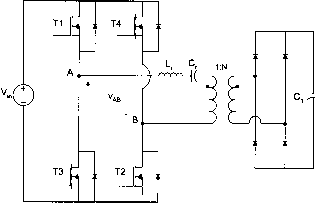 FIGURE 22.7 Series resonant converter. transformer turns ratio of 1:N, reflecting Q through the transformer yields a capacitance of Q. Since N is typically large, this reflected capacitance is much larger than Q; thus, the resonant frequency, which is defined in Eq. (22.10), is not affected by Q. For high-voltage, high-frequency operation, the leakage inductance of the transformer may be utilized as Ц (22.10) One characteristic of this converter that makes it attractive for capacitor charging is the abihty to operate under the short circuit conditions present at the beginning of the charging mode. The voltage across Q is zero at the beginning of this mode. The current flowing in the converter is limited by the input voltage and the impedance Zq, which is defined in Eq. (22.11). The current may be limited to a safe maximum value; however, the charge time will be increased (22.11) Another method for current limiting is to vary the ratio of f, the switching frequency of the MOSFETs, and the resonant frequency, which is co/2n. This effectively controls the flow of energy from the source to Q. The switching frequency may be held constant at some value such as 0.5/. Alternatively, the ratio of to may be set to a low value at the beginning of the charging mode and increased toward 1 as the voltage across Q builds up. This hmits the current when the voltage across Q is low and allows increased energy transfer as the voltage approaches the target voltage. The disadvantage of this approach is that aU circuit components must be designed for variable-frequency operation. The flyback converter [4, 5], shown in Fig. 22.8, also may be utilized for capacitor charging applications. When the MOSFET is turned on, current builds up in the primary N1:N2   FIGURE 22.8 Flyback converter. winding, storing energy in the magnetic field. When it reaches a specified level, the MOSFET is turned off and energy is transferred from the magnetic field to Q. This energy transfer is terminated when the MOSFET is turned on again. Sokal and Redl [4] have investigated different control schemes for charging capacitors using the flyback converter. Their recommendation is to charge Q with current pulses that are nearly flat-topped. This strategy results in higher average current for a given peak current. The capacitor is charged faster, because the charge delivered to it during a pulse is directly proportional to the average current. This desired pulse shape is achieved by turning on the MOSFET to terminate the transfer of energy to Q soon after the MOSFET is turned off. When the primary current reaches the desired level, the MOSFET is again turned off. Another converter for capacitor charging applications is the Ward converter [6-8] shown in Fig. 22.9. When the MOSFET is on, energy is stored in the inductor and capacitor Q transfers energy to the energy storage capacitor Q and capacitor Q. The energy stored in the inductor is transferred to Q when the MOSFET is off. The leakage inductance of the transformer and Q resonate, producing a sinusoidal current that flows in the primary winding of the transformer and the MOSFET. When the primary current reaches zero and starts negative, the diode turns on, which allows the MOSFET to be turned off at zero current. In some converter operating conditions, the voltage across Q is very smaU because most of the energy has been transferred from Q to Q. The energy stored on Q may be too smaU to ensure zero-current turn-off of the MOSFET. In this case, the energy stored on Q helps to ensure that the 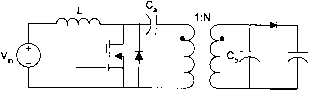 FIGURE 22.9 Ward converter. amplitude of the current is large enough for zero-current turn-off of this device. References 1. p. K. Bhadani, Capacitor-Charging Power Supply for Laser Pulsers Using a Boost Circuit, Review of Scientific Instruments, 60:4, 605-607, (1989). 2. Aaron C. Lippincott and R. M. Nelms, A Capacitor-Charging Power Supply Using a Series-Resonant Topology, Constant On-Time/Variable Frequency Control, and Zero Current Switching, IEEE Transactions on Industrial Electronics, 38:6, 438-447 (1991). 3. B. E. Strickland, M. Garbi, R Cathell, S. Eckhouse, and M. Nelms, 2kJ/sec 25-kV High-Frequency Capacitor-Charging Power Supply Using MOSFET Switches, Proceedings of the 1990 Nineteenth Power Modulator Symposium, June 1990. 4. Nathan O. Sokal and Richard Redl, Control Algorithms and Circuit Designs for Optimally Flyback-Charging an Energy-Storage Capacitor (e.g. for flash lamp or defibrillator), IEEE Transactions on Power Electronics, 12:5, 885-894 (1997). 5. F. P. Dawson and S. B. Dewan, A Subresonant Flyback Converter for Capacitor Charging, Proceedings of the Second Annual IEEE Applied Power Electronics Conference, March 1987, pp. 273-283. 6. Michael A. V Ward, DC to DC Converter Current Pump, U.S. Patent Number 4,868,730, September 1989. 7. George C. Chryssis, High-Frequency Switching Power Supplies: Theory and Design, McGraw-Hill Publishing, New York, 1989. 8. R. M. Nelms and Joe E. Schatz, A Capacitor Charging Power Supply Utilizing a Ward Converter, IEEE Transactions on Industrial Electronics, 39:5, 421-428 (1992). Power Electronics for Renewable Energy Sources C. V. Nayar, Ph.D. S. M. Islam, Ph.D. Centre for Renewable Energy and Sustainable Technologies, Curtin University of Technology, Perth, Western Australia, Australia Hari Sharma, Ph.D. ACRE (Australian CRC for Renewable Energy Ltdj/MUERI, Murdoch University, Perth, Western Australia 23.1 Introduction...................................................................................... 539 23.2 Power Electronics for Photovoltaic Power Systems................................... 540 23.2.1 Basics of Photovoltaics 23.2.2 Types of PV Power Systems 23.2.3 Stand-Alone PV Systems 23.2.4 PV-Diesel Systems 23.2.5 Grid Connected PV Systems 23.3 Power Electronics for Wind Power Systems............................................. 562 23.3.1 Basics of Wind Power 23.3.2 Types of Wind Power Systems 23.3.3 Stand-Alone Wind Energy Systems 23.3.4 Wind-Diesel Hybrid Systems 23.3.5 Grid-Connected Wind Energy Systems 23.3.6 Control of Wind Turbines References.......................................................................................... 572 23.1 Introduction The Kyoto agreement on global reduction of greenhouse gas emissions has prompted renewed interest in renewable energy systems worldwide. Many renewable energy technologies today are well developed, reliable, and cost competitive with the conventional fuel generators. The cost of renewable energy technologies is on a falling trend and is expected to fall further as demand and production increases. There are many renewable energy sources such as biomass, solar, wind, minihydro, and tidal power. However, solar and wind energy systems make use of advanced power electronics technologies and, therefore the focus in this chapter will be on solar photovoltaic and wind power. One of the advantages offered by renewable energy sources is their potential to provide sustainable electricity in areas not served by the conventional power grid. The growing market for renewable energy technologies has resulted in a rapid growth in the need for power electronics. Most of the renewable energy technologies produce dc power, and hence power electronics and control equipment are required to convert the dc into ac power. Inverters are used to convert dc to ac. There are two types of inverters: stand-alone and grid-connected. The two types have several similarities, but are different in terms of control functions. A stand-alone inverter is used in off-grid applications with battery storage. With backup diesel generators (such as PV-diesel hybrid power systems), the inverters may have additional control functions such as operating in parallel with diesel generators and bidirectional operation (battery charging and inverting). Grid-interactive inverters must foUow the voltage and frequency characteristics of the utility-generated power presented on the distribution line. For both types of inverters, the conversion efficiency is a very important consideration. Details of stand-alone and grid-connected inverters for PV and wind applications are discussed in this chapter. Section 23.2 covers stand-alone PV system applications such as battery charging and water pumping for remote areas. This section also discusses power electronic converters suitable for PV-diesel hybrid systems and grid-connected PV for rooftop and large-scale applications. Among aU the renewable energy options, wind-turbine technology is maturing very fast. A marked rise in installed wind power capacity has been noticed worldwide in the last decade. Per-unit generation cost of wind power is now quite comparable with conventional generation. Wind turbine generators are used in stand-alone battery charging applications, in combination with fossil fuel generators as a part of hybrid systems, and as grid-connected systems. As a result of advancements in blade design, generators, power electronics. and control systems, it has been possible to increase dramatically the availability of large-scale wind power. Many wind generators now incorporate speed control mechanisms such as blade pitch control or use converters/inverters to regulate power output from variable speed wind turbines. In Section 23.3, we discuss electrical and power conditioning aspects of wind energy conversion systems. 23.2 Power Electronics for Photovoltaic Power Systems 23.2.1 Basics of Photovoltaics The density of power radiated from the sun (referred to as the solar energy constant ) at the outer atmosphere is 1.373 kW/m. Part of this energy is absorbed and scattered by the earths atmosphere. The final incident sunlight on earths surface has a peak density of 1 kW/m at noon in the tropics. The technology of photovohaics (PV) is essentially concerned with the conversion of this energy into usable electrical form. The basic element of a PV system is the solar ceU. Solar cells can convert the energy of sunlight directly into electricity. Consumer appliances used to provide services such as lighting, water pumping, refrigeration, telecommunications, and television can be run from photovoltaic electricity. Solar ceUs rely on a quantum-mechanical process known as the photovoltaic effect to produce electricity. A typical solar ceU consists of a p-n junction formed in a semiconductor material similar to a diode. Figure 23.1 shows a schematic diagram of the cross section through a crystaUine solar ceU [ 1 ]. It consists of a 0.2-0.3 mm thick monocrystalline or poly-crystaUine silicon wafer having two layers with different electrical properties formed by doping it with other impurities (e.g., boron and phosphorus). An electric field is established at the junction between the negatively doped (using phosphorus atoms) and the positively doped (using boron atoms) silicon layers. If light is incident on the solar ceU, the energy from the light (photons) creates free charge carriers, which are separated by the electrical field. An electrical voltage is generated at the external contacts, so that current can flow when a load is connected. The photocurrent (iph), which is internally generated in the solar ceU, is proportional to the radiation intensity. A simplified equivalent circuit of a solar cell consists of a current source in parallel with a diode as shown in Fig. 23.2a. A variable resistor is connected to the solar ceU generator as a load. When the terminals are short-circuited, the output voltage and also the voltage across the diode are both zero. The entire photocurrent {I) generated by the solar radiation then flows to the output. The solar ceU current has its maximum (4). If the load resistance is increased, which results in an increasing voltage across the p-n junction of the diode, a portion of the current flows through the diode and the output current decreases by the same amount. When the load resistor is open-circuited, the output current is zero and the entire photocurrent flows through the diode. The relationship between current and voltage may be determined from the diode characteristic equation: (23.1) where q is the electron charge, к is the Boltzmann constant, I is photocurrent, Iq is the reverse saturation current, I is diode current, and T is the solar ceU operating temperature (K). The current versus voltage {I-V) of a solar ceU is thus equivalent to an inverted diode characteristic curve shown in Fig. 23.2b. A number of semiconductor materials are suitable for the manufacture of solar cells. The most common types using silicon semiconductor material (Si) are: MonocrystaUine Si cells PolycrystaUine Si cells Amorphous Si ceUs A solar ceU can be operated at any point along its characteristic current-voltage curve, as shown in Fig. 23.3. Two important points on this curve are the open circuit voltage (Vq-) and short-circuit current {I). The open-circuit voltage is the maximum voltage at zero current, whereas the short-circuit current is the maximum current at zero voltage. For a silicon solar ceU under standard test conditions, V is typically 0.6-0.7 V, and is typically 20-40 mA for every square centimeter of the cell area. To a good approximation, is FIGURE 23.1 Principle of the operation of a solar cell [21]. ilph PV CELL illuminated eg. solar cell FIGURE 23.2 Simplified equivalent circuit for a solar cell. 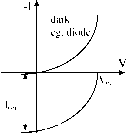 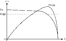 Vmpp Voc figure 23.3 Current vs voltage {I-V) and current vs power {I-P) characteristics for a solar cell. proportional to the iUumination level, whereas V is proportional to the logarithm of the iUumination level. A plot of power (P) against voltage (V) for this device (Fig. 23.3) shows that there is a unique point on the I-V curve at which the solar ceU wiU generate maximum power. This is known as the maximum power point (V, 4ip). To maximize the power output, steps are usually taken during fabrication to maximize the three basic ceU parameters: open-circuit voltage, short-circuit current, and fiU factor (FF) - a term describing how square the /- V curve is, given by Fill factor = (V p/ p)/(Voc4c) (23.2) For a sUicon solar ceU, FF is typically 0.6-0.8. Because sUicon solar ceUs typically produce only about 0.5 V, a number of cells are connected in series in a PV module. A panel is a coUection of modules physically and electrically grouped together on a support structure. An array is a collection of panels (see Fig. 23.4). The effect of temperature on the performance of a sihcon solar module is iUustrated in Fig. 23.5. Note that I shghtly increases hnearly with temperature, but V and the maximum power P decrease with temperature [1]. Figure 23.6 shows the variation of PV current and voltages at different insolation levels. From Figs. 23.5 and 23.6, it can be seen that the I-V characteristics of solar ceUs at a given insolation and temperature consist of a constant-voltage segment and a constant-current segment [2]. The current is limited, as the ceU is short-circuited. The maximum power PV с ell PV M odule P V Panel PV Array 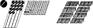 figure 23.4 PV generator terms. condition occurs at the knee of the characteristic where the two segments meet. 23.2.2 Types of PV Power Systems Photovoltaic power systems can be classified as foUows: Stand-alone Fiybrid Grid connected Stand-alone PV systems, shown in Fig. 23.7a, are used in remote areas with no access to a utility grid. Conventional power systems used in remote areas often based on manually controUed diesel generators operating continuously or for a few hours. Extended operation of diesel generators at low load levels significantly increases maintenance costs and reduces their useful life. Renewable energy sources such as PV can be added to remote area power systems using diesel and other fossU fuel powered generators to provide 24-hour power economically and efficiently. Such systems are caUed hybrid energy systems. Figure 23.7b shows a schematic of a PV-diesel hybrid system. In grid-connected PV systems, as shown in Fig. 23.7c, PV panels are connected to a grid through inverters without battery storage. These systems can be classified as smaU systems, such as residential rooftop systems or large grid-connected systems. The grid interactive inverters must be synchronized with the grid in terms of voltage and frequency. 23.2.3 Stand-Alone PV Systems The two main stand-alone PV applications are: Battery charging Solar water pumping 23.2.3.1 Battery Charging 23.2.3.Ll Batteries for PV Systems A stand-alone photovoltaic energy system requires storage to meet the energy demand during periods of low solar irradiation and nighttime. Several types of batteries are avaUable, such as lead-acid, nickel-cadmium, lithium, zinc bromide, zinc chloride, sodium-sulfur, nickel-hydrogen, redox and vanadium batteries. The provision of cost-effective electrical energy storage remains one of the major challenges for the development of improved PV power systems. Typically, lead-acid batteries are used to guarantee several hours to a few days of energy storage. Their reasonable cost and general avaUability has resulted in the widespread application of lead-acid batteries for remote area power supplies despite their limited lifetime compared to other system components. Lead acid batteries can be deep or shallow cycling, geUed batteries, batteries with captive or hquid electrolyte, sealed and nonsealed batteries, etc. [3]. Sealed batteries are valve regu- Current in A 3.5 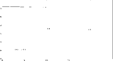 Voltage in V FIGURE 23.5 Effects of temperature on silicon solar cells. lated to permit evolution of excess hydrogen gas (although catalytic converters are used to convert as much evolved hydrogen and oxygen back to water as possible). Sealed batteries need less maintenance. The foUowing factors are considered in the selection of batteries for PV applications [ 1 ]: Deep discharge (70-80% depth discharge) Low charging/discharging current Long-duration charge (slow) and discharge (long duty cycle) Irregular and varying charge/discharge Low self-discharge Long lifetime Less maintenance requirement High energy storage efficiency Low cost Battery manufacturers specify the nominal number of complete charge and discharge cycles as a function of the depth-of-discharge (DOD), as shown in Fig. 23.8. Although this information can be used reliably to predict the lifetime of lead-acid batteries in conventional apphcations, such as unin-terruptable power supplies or electric vehicles, it usually results in an overestimation of the useful life of the battery bank in renewable energy systems. Two of the main factors that have been identified as limiting criteria for the cycle life of batteries in photovoltaic power systems are incomplete charging and prolonged operation at a low state-of-charge (SOC). The objective of improved battery control strategies is to extend the lifetime of lead-acid batteries to achieve the typical number of cycles shown in Fig. 23.8. If this is achieved, an optimum solution for the required storage capacity and the maximum depth-of-discharge of the battery can be found by referring to the manufacturers information. Increasing the capacity wiU reduce the typical depth-of-discharge and therefore prolong the battery lifetime. Conversely, it may be more economic to replace a smaUer battery bank more frequently. 23,23,1,2 PV Charge Controllers Blocking diodes in series with PV modules are used to prevent the batteries from being Current in A 100% Insolation SO% Insolatio eO°y& Insolation AO°A> Insolatic 20% Insolation  1 О Voltage in V FIGURE 23.6 Typical current/voltage (/- V) characteristic curves for different insolation levels. 1 ... 51 52 53 54 55 56 57 ... 91 |
||||||||||||||||||||||||||||||||
|
© 2026 AutoElektrix.ru
Частичное копирование материалов разрешено при условии активной ссылки |