 |
 |
 |
| Главная Журналы Популярное Audi - почему их так назвали? Как появилась марка Bmw? Откуда появился Lexus? Достижения и устремления Mercedes-Benz Первые модели Chevrolet Электромобиль Nissan Leaf |
Главная » Журналы » Metal oxide semiconductor 1 ... 58 59 60 61 62 63 64 ... 91 FIGURE 25.6 Static VAR compensation using TSC and TCI. From this, we see that the maximum amphtude of occurs for a = я/2 and is equal to V/cdL = /iV/cdL. This corresponds to an rms value of V/cdL. The minimum value is zero at a = Я. Between these hmits, the lagging current and so the lagging reactive VA are adjustable by variation of a. 25.2.4.5 Static VAR Compensation Circuit Figure 25.6 shows the typical method of static VAR compensation. The leading reactive current necessary for VAR compensation is actually supphed by connecting capacitor banks across the ac hnes. Before the development of thyristors, this was done using electromechanical circuit breakers. With the advent of thyristors, bidirectional ac switches using them were developed for connecting and disconnecting the capacitor banks. A capacitor bank connected in this way is caUed a thyristor-switched capacitor (TSC). The problem to be faced when connecting the capacitor to the high-voltage lines is the large inrush current that will flow at the moment of contact if there is a large instantaneous voltage differential between the line and the capacitor. It is relatively easy to overcome this difficulty, because the TSC uses static thyristor switches that can be gated at any desired instant in an ac cycle by means of a switching controUer that wiU sense the voltage differential and gate the thyristor at the correct instant in the ac cycle when the voltage differential is within permissible hmits. If only TSCs are employed for VAR compensation, the leading VAR to be introduced can only be adjusted in steps, because the switching is to be done one capacitor bank at a time. For precise adjustments of VAR, as dictated by the system requirements, a continually variable feature is desirable. This is achieved in the scheme in Fig. 25.6 by having a thyristor-controUed reactor in paraUel with the capacitor bank. If the maximum lagging current drawn by the TCI is equal to the leading reactive VA of the capacitor, the two wiU cancel and the net reactive VA wiU be zero. From this point, the lagging VAR of the TCI can be progressively decreased by phase control, thereby increasing the net leading VAR. After the maximum is reached, a further increase can be made by switching in another capacitor bank. In this manner, the TSCs provide VAR in steps, whUe the TCI wiU provide the continuous adjustment between steps. This scheme enables precise and fast automatic adjustment of the VAR by means of closed-loop control. A practical system wiU be invariably a three-phase network, although we have used the single-phase equivalent to describe the technique. Also, in a practical high-voltage system the TSCs and TCIs may be connected to the secondary side of a transformer. In this way, the maximum voltage requirements of the thyristors and the capacitors can be lowered. 25.3 Modeling and Analysis of an Advanced Static VAR Compensator After introducing classical methods for compensating the reactive power, we propose a new concept, the advanced static VAR compensator [14], based on the exact equivalence with the classical rotating synchronous compensator. This type of compensator uses a source voltage type inverter with a capacitor in the dc side used as energy storage element. First a modeling and analysis of the compensator, which uses a programmed PWM with a constant conversion ratio, is undertaken. Then, the dynamic behavior of the system in the open-loop condition wiU be identified. Moreover, we apply this new concept of advanced static VAR compensation to improve the StabUity of a power system network, and prove this through a series of simulation tests. The proposed ASVC system is modeled using the d - q transform [7] and employs a programmed PWM voltage wave-shaping pattern, which can be easily stored in an EPROM to simphfy the logic software and hardware requirements. The programmed PWM has the advantage that there are fewer harmonic components in the current, a better power factor, and lower switching frequencies, and thus less stress on switching devices and reduction of switching losses. At first, an identification of the dynamic behavior of the system in open loop wiU be the key to the synthesis of such an approach to control, and it wiU be shown that this control approach is more efficient for industry applications [15-16]. The control of the static VAR compensator (ASVC) system with self-controlled dc bus, which employs a three-phase PWM voltage source inverter, wiU be modeled and analyzed. Such an SVC is made up of a two-level voltage-source inverter and presents a fast response time and reduced harmonic poUution. 25.3.1 Main Operating Principles of the ASVC 25.3.1.1 Main Circuit Configuration The major ASVC system component is a three-phase PWM forced commutated voltage source inverter as shown in FIGURE 25.7 Main circuit of ASVC. FIGURE 25.10 ASVC single phase diagram as a combination of two converters. Figure 25.8 shows a simphfied equivalent circuit of the ASVC. In this representation, the series inductance Ц accounts for the leakage of the transformer and represents the active losses of the inverter and transformer. С is the capacitor on the dc side. The inverter is assumed to be lossless. V and V are the amplitude of the fundamental of the output voltage of the converter and phase voltage of the supply, respectively. FIGURE 25.8 Equivalent circuit. Fig. 25.7. The ac terminals of the inverter are connected to the ac mains through a first-order low-pass filter. Its function is to minimize the damping of current harmonics on utility lines. The dc side of the converter system is connected to a dc capacitor, which carries the input ripple current of the inverter and is the main reactive energy storage element. The dc supply provides a constant dc voltage and the real power necessary to cover the losses of the system. 25.3.1.2 Operating Principles The operating principles of the ASVC can be explained by using its equivalent single-phase circuit given by Fig. 25.9, which is inherently a combination of two converters as shown in Fig. 25.10 after rearrangement of the circuit of Fig. 25.9. If the fundamental component of the output voltage of the inverter V is in phase with the supply voltage V, the current flowing out the ASVC or toward the ASVC is always at 90° to the network voltage because of reactive coupling. According to the circuit shown in Fig. 25.10, converter 1 operates as an uncontrollable rectifier through which a small quantity of real power flows from the ac to dc side, and converter 2 operates as an inverter when the real power flows in the reverse direction. Initially, when the converter 2 is not conducting, the capacitor С is charged up to the peak value of supply voltage through converter 1, and remains at this voltage for as long as there is no real power transfer between the circuit and the supply. If the switches of converter 2 are operated to obtain the fundamental of the ASVC output voltage slightly leading the ac main voltage, converter 2 conducts for a superior period to the FIGURE 25.9 Equivalent single-phase circuit of the ASVC. FIGURE 25.11 Phasor diagram for leading and lagging mode. one of the converter 1, causing a transfer of real power from the dc side to the ac side. In this way the dc capacitor voltage is decreased, and a reactive power is absorbed by the ASVC system (lagging mode). The inverse is true when the fundamental of the ASVC output voltage slightly lags the supply vohage: The dc capacitor voltage is increased, and a reactive power is generated by the ASVC (leading mode). We can conclude that the reactive power either generated or absorbed by the ASVC can be controlled only by one parameter: the phase angle between the ASVC output voltage and the supply voltage. Thus, as indicated by the phasor diagram shown in Fig. 25.11, when the amplitude of the inverter output voltage is smaller than the supply voltage V, the reactive power is absorbed by the ASVC. Otherwise, the ASVC generates the reactive power when the amplitude of the supply voltage is larger than the output voltage of the inverter. 25.3.2 Modeling of the ASVC System To achieve an easier modeling of the system [24], the original circuit is subdivided in several basic subcircuits as shown in Fig. 25.8. 25.3.2.1 Transform of Part A The three-phase supply voltages are given by the foUowing equation: The d - q transform of (25.3) yields s,qdo = s\do + qdo (25.4) 25.3.2.3 Transform of Part С The relationship between the voltage and the current in the part of inductor is -iabc) - abc ~ o,abc The d - q transform of (25.5) yields Assembling parts В and C: d dt CO--- Vsd - Vod (25.5) Ls(iqdo) = iK)K ia, + va, - (25.6) (25.7) (25.8) (25.9)
where a is the phase angle difference between the source voltages and those of the inverter. In the d - q frame: - sma cos a 0 (25.2) With: cos(cot) cos(cot - 2n/3) cos(cot-\-2n/3) sin(a;t) sin(a;t - 2n/3 sin(a;t -h 2я/3) 1/V2 1/V2 1/V2 25.3.2.2 Transform of Part В The relationship between the voltage and the current in the part of the resistor = Rsabc + (25.3) 25.3.2.4 Transform of Parts D and E Under the assumption that harmonic components generated by the switching pattern are negligible, the switching function S can be defined as foUows:
The modulation index, being constant for a programmed PWM, is given by: = o,peak/dc = VVni The inverter output voltages are given by o,abc = SVdc In the d - q axis: (25.11) (25.12) o,qdo = KSv = m (25.13) So Eq. 25.9 can be written as follows: From equation system (25.20), we can extricate the following expressions: d Jt - sin a cos a - mv The dc side current in the capacitor is given by cT Uc - hbc In the d - q axis z = s:-g = m[o 1 0] (25.14) (25.15) (25.16) (25.17) Ш = -+ p -sma+-cosa +-sma Рз + 2р2 + р( 2 + ЦС (25.21) cos a /J, CO . \ p, - + p[-cosa--sшay Pi + 2p2 R, / R R, , cos a R, CO p-TTT + TTcosa -sma R, ( Ri m. (25.23) Expressions of real and reactive power are given by The relationship between the voltage and the current in the dc side is given by: Pc(p) = Vsqiq + = - V,(i sin a - jrf cos a) (25.24) чЛР) = sq4 - Vsdiq = - Vsiid sin + iq cos a) (25.25) Thus, replacing Eq. (25.17) in (25.18), we will have: (25.18) 25.3.3 The ASVC Behavior in Steady State Equations governing the steady-state behavior of the ASVC can be obtained by equating the term of derivatives in the mathematical model given by Eq. (25.20) to zero, which is similar to short-circuiting the inductors and opening the capacitor, so we will have: dt С (25.19) Collecting all parts of the system, while introducing the third equation (25.19) (the model of the dc part in the system), the complete mathematical model of the ASVC in the d - q axis will be as follows: Ч Ч
Ч - sma cos a 0 V, sin a 4 = dc = - I cosa--sma m \ Pc 4c sin a Vf sin a cos a (25.26) (25.27) (25.28) (25.29) (25.30) (25.20) We note that the active and reactive power depend only on the square of the supply voltage and the resistor of coupling of the ASVC to the ac mains, and are independent of the other parameters of the circuits (Lj and C). In addition, the dc side 600 500 400 300 200 100 0 -100 -200
10 20 -30 -20 -10 0 FIGURE 25.12 Steady-state values. q [kvar] p [kw] 30 20 -30 -20 -10 0 10 20 FIGURE 25.13 Real, reactive power in steady state. voltage depends on a, the modulation index, and the resistor and inductor of the coupling, but is independent of the value of the dc capacitor. The system parameters are given by Supply: V, = 220 V, / = 50 Hz, R, = I Q, = 5 mH DC side: С = 500F m = 1.12/л/з By varying the angle a in an interval of -30° to +30° which is the linear zone for sine and cosine, we obtain the following responses. Figure 25.12 shows i, ij, and v values for different values of a, where we can note that the real current is always zero; on the other hand, the reactive current and the dc voltage v are linear according to a. Figure 25.13 shows the real and the reactive power flowing from or to the ASVC for different values of a, where it is clear that the reactive power has a linear variation according to a, and the real power always exists to cover the losses in the system and to maintain the dc side voltage at the operating level. 25.3.4 ASVC Behavior in Transient State Taking as an initial condition for the dc side voltage the maximum voltage of the supply, a series of dynamic responses of the system to step changes of ±10° of the angle a have been established [17]: Figure 25.14 shows the response of the reactive current to a step change of a = -10° for Fig. 25.14a and a = +10° for Fig. 25.14b, which after a short transient state attains a stable value of 38 A supphed to the network. Figure 25.15 shows the response of the dc side voltage v to a step change of (a = -10° for Fig. 25.15a and a = +10° for Fig. 25.15b, in which attains a value greater than that of the network: capacitive mode. Figure 25.16 shows the response of the active current (a = -10° for Fig. 25.16a and a = +10° for Fig. 25.16b), which, after the voltage v reaches its stable value, it goes to zero, because its action on the transient state is only for charging and discharging the dc side capacitor. Figure iq[a] 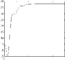 0.02 0.04 0.06 0.08 0.1 temps [s] FIGURE 25.14 Transient reactive current response. FIGURE 25.15 Active current response to change of a. FIGURE 25.16 Dc side vohage response to change of a (°). FIGURE 25.17 Reactive power response to change of a. TABLE 25.1 Switching angles
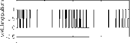 0.005 0.01 0.015 0.02 time (sec) 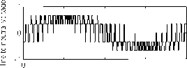 0.005 0.01 0.015 0.02 time (sec) FIGURE 25.18 Switching pattern and line to neutral voltage. 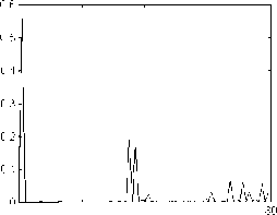 0 20 40 60 Harmonic rank FIGURE 25.19 Harmonic spectrum of line-neutral voltage. The advantages of this programmed PWM over the classical PWM are as foUows: 1. Nearly 50% reduction of switching frequency 2. PossibUity of high voltage gain due to overmodulation 3. Dc side-current ripples low because of high quality of current and voltage waveforms 4. Reduction of the PWM frequency, which lowers the switching losses and thus can be used for high-power applications 5. Elimination of low-order harmonics, which aUows avoiding resonance. 25.3.5 Controller Design The controUer design of the ASVC is based on the linearized model of the system under the foUowing assumptions: Disturbance ад is smaU. The second-order terms are dropped. The quiescent operating is near zero. The trigonometric nonlinearities are treated as follows: cos(ao + ад) = cos ag cos ад - sin sin ад sin(ao + ад) = cos sin ад + sin ag cos ад (25.31) After development and simplification, the linearized model in state space is given by Хд=АХд + Б[/д (25.32) 25.17 shows the behavior of the reactive power to a step change of a = -10° for Fig. 25.17a and a = +10° for Fig. 25.17b), which after two cycles reaches a stable value of -8.47 kVar supphed to the network capacitive mode and +8.47 kVar for the inductive mode. A programmed PWM switching pattern, which aUows the ehmination of a selected number of harmonics, is continuously applied to the six controlled switches (Table 25.1). This method is used because it offers better voltage utUisation and lower switching frequencies, and thus less stress on switching devices and reduction of the switching losses (increase of the efficiency of the converter). For our work, we use a programmed PWM with the parameters given by MI (modulation index) = 1.12. Figure 25.18 shows the switching pattern, and the corresponding line to neutral output inverter voltage. Figure 25.19 shows the harmonic spectrum of the output inverter voltage, where it is clear that the elimination of harmonics is verified. with
Г Vl Ls 0 0 0] FIGURE 25.22 Details of the control block diagram. FIGURE 25.20 PI design criteria by root locus. The transfer function relating the reactive power to the angle д is given by The closed-loop transfer function of PI associated with the transfer function of the ASVC is given by FpiG 1 + FpiG (25.35) G(P) = =Q[pJ-A]-B G(p) = ,Rs ( , R] пг\ 2 Rs (25.33) If we take = 0.003, Fig. 25.20 shows the root locus for К varying from zero to infinity. The value of К that gives us a closed loop response with a damping factor С = 0.7 is iC = 7.5 X 10 Thus the PI controller is conceived so that the ASVC has a desired dynamic performance. The PI transfer function is Ыр) = 1 + (25.34) FIGURE 25.23 Simulated reactive power response. FIGURE 25.21 Main and control circuit for the proposed system. FIGURE 25.24 Simulated current and voltage waveforms. Computer simulation was carried out using Matlab, with the system parameters given by Supply: V, = 220 V, / = 50 Hz, i, = 1 Q, Ц = 5 mH; dc side: С = 500 F; PI controller: Kp = 7.5 x 10 Kj = 2.5 x 10 FIGURE 25.25 Simulated inverter dc bus voltage. The parameters of the PI controUer are Kp = K = 7.5x 10 Kj = = 2.5 x 10- 25.3.6 Proposed Control Block Diagram Figure 25.21 shows the main control circuit of the system, representing the different blocks constituting the control system. DetaUs of the control block are iUustrated by Fig. 25.22. The source voltage and the ASVC currents are transformed in the d - q axis for calculating the reactive power generated by the system, which is compared to the reference; the vector PEL detects the phase angle of the supply, which is added to the control variable a (output of the PI controller). This sum adjusts the reading frequency of the counter connected to the EPROM where the switching pattern is stored. To verify key analytical results and the validity of the proposed control scheme [10,18], the aforementioned ASVC structure was tested on a Pentium personal computer. Testing of the ASVC system shown in Fig. 25.21 was performed for dynamic response. The amplitude of the reference was adjusted to cause the system to swing from leading to lagging mode. Figure 25.23 shows the simulated reactive power response to a reference change from lOkVar lagging to lOkVar leading. Performance evaluation of the subject model was also tested for current and voltage responses to step changes. Figure 25.24 shows the simulated current and voltage waveforms to a step reference change from 10 kVar lagging to 10 kVar; leading, this figure confirms that the compensator time response is fast (about 10 ms). The dc side voltage response to the same change is depicted in Fig. 25.25. Figure 25.26 shows the simulated inverted output voltage and voltage source waveforms to a step reference change from 10 kVar lagging to 10 kVar leading and how the inverter output voltage responds during transients. 25.3.7 Conclusion A new model of advanced static VAR compensator has been developed. A fast control approach of the ASVC system has been implemented for applications that require leading or lagging power compensation. The proposed control strategy is based on an explicit control of the reactive power implicit in the voltage amplitude of the capacitor of the dc side and is more flexible. The simulation results show that this control strategy has good dynamic performance for generating or consuming of the reactive power. FIGURE 25.26 Simulated inverter line to neutral and source voltage. FIGURE 25.27 Schematic diagram of the network ASVC. 25.4 Static VAR Compensator for the Improvement of Stability of a Turbo Alternator The requirement to design and operate power systems with the highest degree of efficiency, security, and rehability has been the central focus for the power system designer ever since interconnected networks came into existence. To satisfy these requirements, various advances in the technology of ac power transmission have taken place in the context of effective control of reactive power and its compensation. The static VAR compensator (SVCs ) is a dynamic reactive power compensation device. Recent developments in sohd-state VAR compensators have led to the hope of achieving very efficient control of reactive power. This stems from the fact that the voltage is maintained constant within a specified level, to improve the dynamic stability of the power system and its power factor as well as correcting the phase unbalance. In this section, we will study the case when disturbances occur at the studied machine without affecting the behavior of the other machines (that is, speed and emf are constants). This means that the voltage and frequency of the network can be considered constant. The turbo-alternator is then connected to a distribution network called infinite. 25.4.1 Mathematical Model of the Network ASVC Based on Fig. 25.27 we can establish the following equations: Machine side: Network side: yrd = yd- RUl - LpidL - Lcoil - LiqLp rq =\- - LpiqL + Lcoil + LlLp ASVC side: РЧс = Pkc = with d - Rs4c - Lspidc - LsCoiqc q - Rs\C - LspiqC + sJC --YVd-ycd-Rsidc-LsCoic] Yyq-yCq-RJqCL.CDiac] Ы - dA ~ dC (25.36) (25.37) (25.38) (25.39) (25.40) A. Diaou, M. Benghanem, and A. Tahri By putting (25.40) into (25.37), we get Vrd = yd- R(Ua - idc) - LpiUA - idc) - LcoOqA - \c) - Ща - \c)P Kq =\- Ща - \C) - LpiqA + Lplc - LcoOdA - 4c) - L(dA - 4c)P (25.41) By developing (25.41) and replacing by (25.39) and after a tedious calculation, we obtain the complete model of the infinite bus bar network with ASVC (or ASVC) : V2v, sin 3 -(Ик+ + )+к\ \ \ do do/ / -(o(L + F\j, -d + Vf + Xic Vdo do/ /(i+A) (25.42) -v,cosS-{dR,+ - ]+R]i Ф /(L+F) (25 A3)
with =(1+1 and Я=и-4 The model of the ASVC is established by taking the voltage of the bus bar as a reference. Hence, we get Cdqo = KSv = m sma cosa 0 (25.49) 1 ... 58 59 60 61 62 63 64 ... 91 |
|
© 2026 AutoElektrix.ru
Частичное копирование материалов разрешено при условии активной ссылки |