 |
 |
 |
| Главная Журналы Популярное Audi - почему их так назвали? Как появилась марка Bmw? Откуда появился Lexus? Достижения и устремления Mercedes-Benz Первые модели Chevrolet Электромобиль Nissan Leaf |
Главная » Журналы » Metal oxide semiconductor 1 ... 59 60 61 62 63 64 65 ... 91 FIGURE 25.28 Main circuit of the control strategy. Thus, the model of the ASVC is given as РЧс = (-RsUc - s\c - dc sin(a,) + v)/L (25.53) Pkc = (-Rskc - hhc - dc cos(a,) + v)/L (25.54) Pdc = Hhc sin(a,) + cos(a,))/C (25.55) with = a + , since we have taken the voltage of the bus bar as a reference for the ASVC, i.e., on the phasor diagram the voltages of the ASVC are synchronized to those of the bus bar considered. Fience, our model wiU be made up of 10 differential equations, seven for the alternator and three for the ASVC. For the initialization of the system, we take for the machine the same conditions given in [13-21], and for the ASVC the following initial conditions: FIGURE 25.29 Details of the control block. with
25.4.2 Proposed Control Strategy Figure 25.28 shows the main principles of the proposed control of the ASVC: the reactive power demanded is always compensated partly by the capacitive reactive power generated by the ASVC. This method of compensation help ease the alternator and increase the security boundary for the heating of the rotor circuit. Figure 25.29 gives the details of the control block diagram. The reactive power demanded, being inductive, must be compensated by the capacitive reactive power generated by the ASVC. A PI regulator controls this compensation, which synthesizes the control variable a, which is added to the angle д that is necessary for synchronizing with the voltages of the bus bar considered. This sum, being a, is apphed to the ASVC to The current of the dc side capacitor is given (in the Park axis) by ij, = SK i = m(iq sin a + cos a) (25.51) Fience, the dc side voltage is given by dc = (kc + dc cos a) (25.52) FIGURE 25.30 Load angle variation. generate the necessary reactive power; the control variable a is limited by two upper and lower levels, which allows preserving the stability of the compensator. If we suppose that the reference is always the voltage of the bus bar connected to the ASVC, the transfer function relating the reactive power to the control angle a is given by [17] G(p) = (P) >2 Rs ( 2 R] 2 Rs FIGURE 25.31 Variation of the angular speed. As for the PI regulator, it is designed similarly as given in Section 25.2, with the same constant of time of integration, but the voltage level will change. Hence, by using the root-locus method, the parameters of the regulator are given as follows: Kp = 2.3 X 10- Kj = 7.7 X 10 FIGURE 25.32 Variation of the vohage of the first bus bar. FIGURE 25.33 Load angle variation of the turbo-alternator. 25.4.3 Simulation Results To analyse the performance of the stability of the turbo-alternator with ASVC, a series of simulation tests have been carried out, by taking the compensator parameters as follows: ac side: i = 1 Q, 4 = 5 mH; dc side: С = 500 F. The results obtained for the turbo alternator and ASVC are compared with those of the turbo alternator alone. Figure 25.30 represents the variation of the load angle of the turbo alternator group with and without compensation after clearing the fault of 0.08 s. We notice that the response with the compensation is more damped and the load angle is smaller than that of the turbo alternator without compensation. Figure 25.31 represents the variation of the angular speed centered on the turbo alternator with and without compensation after clearing the fault of 0.08 s. We notice that the response with compensation is more damped than without compensation. Figure 25.32 represents the variation of the voltage of the first bus bar with and without compensation. The voltage of the compensated system is higher than that without compensation. This is due to the decrease in reactive power in the lines by the ASVC, which generates a capacitive reactive current that nullifies a part of the inductive reactive current absorbed by the hne. Figure 25.33 shows the variation of the load angle of the turbo-alternator with and without compensation after the clearing of the fault of 0.3 s, which is the critical time for clearing the fault for the alternator without compensation. We notice that the introduction of the ASVC has allowed improvement of this clearing time and an increase in the level of stability of the system. 25.4.4 Conclusion In this section a new approach to improve the stability of a turbo-alternator using static VAR compensator has been presented. The mathematical model derived and the transient simulated results obtained are included to confirm the apphc-ability of the proposed control scheme. This control approach is more suitable for industrial applications, which require continuous control of the reactive power. Analysis of the simulation results aUows us to conclude that the use of the inverter as a compensator of reactive power brings better performance than classical methods and gives to the electro-energetic system better flexibility. 25.5 Multilevel Inverters Recent advances in the power-handling capabilities of static switch devices such as IGBTs with voltage rating up to 4.5 kV commercially available, has made the use of the voltage source inverters (VSI) feasible for high-power apphcations. High-power and high-voltage conversion systems have become very important issues for the power electronic industry handling the large ac drive and electrical power applications at both the transmission and distribution levels. As a result, a variety of VSI-based equipment such as static compensators (STATCOM) is used to make flexible ac transmission systems (FACTS) possible. The ability of this FACTS equipment to control reactive power systems as well as to improve system stability may required the use of VSI with high-voltage and high-power capabilities. This is not possible for a two-level inverter, as the semiconductor devices must be connected in series to obtain the required high-voltage operation. This can be achieved by summing the outputs of several two-level converters with transformers or inductors, or direct series connection, or by more complex topologies such as the diode clamped inverter and the flying capacitor inverter. The multilevel pulse-width modulation (PWM) converter topology has drawn tremendous interest in the power industry since it can easily provide the high-power required for high-power applications for such uses as static VAR compensation and active power filters, and so that large motors can also be controlled by high-power adjustable-frequency drives. The most popular structure proposed as a transformerless voltage source inverter is the diode-clamped converter based on the neutral point clamped (NPC) converter proposed by Nabae et al. [22]. It has the advantages that the blocking voltage of each switching device is one-half of the dc hnk voltage and the harmonics contents output voltage is far less than those of two-level inverters at the same switching frequency. A general trend of replacing existing conventional inverter by neutral point clamped (NPC) inverters in high-power applications is taking place. The multilevel voltage source inverters unique structure aUows them to reach high voltages with low harmo- FIGURE 25.34 transformers. Schematic diagram of an inverter with 6V pulses by nics without the use of transformers or series-connected synchronized switching devices, a benefit that many contributors have been trying to appropriate for high-voltage, high-power applications. The general structure of the multilevel converter, which has a multiple of the usual six switches found in a three-phase inverter, is to synthesize a sinusoidal voltage from several levels of voltages, typically obtained from capacitor voltage sources. The main motivation for such converters is that current is shared among these multiple switches, aUowing a higher converter power rating than the individual switch VA rating would otherwise allow with low harmonics. As the number of levels increases, the synthesized output waveform, a staircaselike wave, approaches a desired waveform with decreasing harmonic distortion, approaching zero as the number of levels increases. The structure of the multUevel inverter starts from three-level, also known as a neutral clamped converter [23-25], and consists of two capacitor voltages in series and uses the center tap as the neutral. Each phase leg of the three-level converters has two pairs of switching devices in series. The center of each device pair is clamped to the neutral through clamping diodes. The waveform obtained from the three-level converters is a quasi-square-wave output. 25.5.1 Different Structures of the Multilevel Inverters There are roughly three main types of transformerless multilevel inverter topologies, which have been studied and received considerable interest from high-power inverter system manufacturers: the flying-capacitor inverter, the diode-clamped inverter, and the cascaded H-bridge inverter. A detaUed overview and comparison of characteristics and their implementa- FIGURE 25.35 Schematic diagram of: (a) one leg of converter; (b) three-level converter; (c) one leg of M multilevel converter. TABLE 25.2 States of the switches for one leg of converter
tion issues is given next. All share the same property, which is that the output filter can be dramatically reduced, and the usual bandwidth limit induced by the switching frequency can be reconsidered. FIGURE 25.36 Switching states. 25.5.1.1 Multilevel Inverters with Transformer An inverter with M levels that has P = 6M pulses is obtained from an inverter with six pulses at the fundamental thanks to the following operating structure. We operate the inverters through a common dc source with successive phase displacement of 2n/6M. 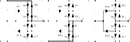 FIGURE 25.37 Current flow. The transformer secondary windings have appropriate configurations and connections to obtain the three-phase voltage by connecting the primary winding of the transformer in series and paraUel, which displaces each waveform of the output voltage likewise obtained. Figure 25.34 shows a model with N pulses used as reactive power generator (SVG) made of eight (8) inverters with six (6) pulses using the transformers with particular connection so to ehminate harmonics and reduce the total harmonic distortion. This first type of multilevel inverter presents the foUowing drawbacks: 1. Total pricing of the system is related mainly to the transformers used. 2. They produce roughly 50% of the total losses of the system. 3. They occupy 40% of the total surface aUowed for the system. 4. They make the control difficult because of problems related to overvoltages caused by saturation in the transient state. 25.5.1.2 Neutral-Point-Clamped Inverter Figure 25.35a shows a schematic diagram of the structure of a three-level (Neutral-point clamped) inverter. It may be coupled directly to a level of voltage of 3.3 kV by using a GTO of 4.5 kV [26, 27]. Taking for reference one leg of the converter as shown in Fig. 25.35b, Table 25.2 gives overaU switching states of the GTO, to obtain the voltages 0, £/2, and E three (3) states per leg; thus, for a three-phase converter there are 27 states in total. Figure 25.36 shows a structure of an M multUevel converter; in this case we use (M - 1) x 2 x 3 GTO, (M - 1) x 2 x 3 diodes in anti-paraUel, (M - 1) x (M - 2) x 3 clamping diodes, and (M - 1) capacitors. Figure 25.37 represents the transitions of the switches of one leg according to the indicated states in Table 25.2. Figure 25.37 also shows the direction of the current flow for each state. (Sll, S14); (S21, S24); (S31, S34) are the main switches; they are switched directly by control pulses. (S12, S13); (S22, S23); (S32, S33) are the auxiliary switches and allow connection of the output of each phase to neutral point (0). (Dll-D32) intervene in this operation. As an example, for M = 51 for a direct connection with a 69-kV network, 300 GTOs and diodes in antiparallel, 50 capacitors, and 7350 clamping diodes are needed. This second type of converter presents the following advantages: 1. When M is very high, the distortion level is so low that the use of filters is unnecessary. 2. Constraints on the switches are low because the switching frequency may be lower than 500 Fiz (there is a possibility of switching at the line frequency). 3. Reactive power flow can be controUed. The main disadvantages are: 1. The number of diodes becomes excessively high with the increase in level. 2. It is more difficult to control the power flow of each converter. FIGURE 25.38 converter. Schematic diagram of a three-level flying capacitor type 25.5.1.3 Flying Capacitors Figure 25.38 shows the structure of a flying-capacitor type converter. We notice that compared to NPC-type converters a high number of auxUiary capacitors are needed, for M level (M - 1) main capacitors and (M - 1) x (M - 2)/2 auxiliary capacitors. The main advantages of this type of converter are: Val Va(s-l) ± 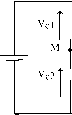 j3 ;iJ Vbl i Vb2 i j3 Jin j3 Ji* Vb(s-l) Vbs j3 j!*
Vcl Vc2 i ;3 JL Vc(s-l) ZZ Vcs FIGURE 25.39 Schematic diagram of a 9-level cascaded-type converter. ]lj m
JLi Jii
4= с S11 S21 ЛЛПГ ЛГГГ S31 S41 FIGURE 25.40 Topology of a three-level inverter. 1. It uses fewer components than the other types. 2. It has a simple control, since the converters present the same structure. However, the main drawback is that it needs separate dc sources for the conversion of the active power, which limits its use. 1. For a high M level, the use of a filter is unnecessary. 2. Control of active and reactive power flow is possible. The drawbacks are: 1. The number of capacitors is very high. 2. Control of the system becomes difficult with the increase of M. 25.5.1.4 Cascaded-Type Multilevel Inverter Figure 25.39 represents the structure of a three-phase cascaded-type converter with separate dc sources; it shows an example of a 9-level converter. This type of converter does not need any transformer clamping diodes, or flying capacitors; each bridge converter generates three levels of voltages (£, 0, and -E). For a three-phase configuration, the cascaded converters can be connected in star or delta. It has the following advantages: 25.5.2 Conclusion Among these inverter topologies, the flying capacitor inverter is difficult to realize because each capacitor must be charged with different voltages as the voltage level increases. Moreover, the diode-clamped inverter is difficult to expand to multilevel because of the natural problem of the dc hnk voltage unbalancing, the increase in the number of clamping diodes, and the difficulty of the disposition between the dc link capacitors and the devices as the voltage increases. Though the cascaded inverter has the disadvantage of needing separate dc sources, the modularized circuit layout and package are possible, and the problem of the dc link voltage unbalancing is not occurred. Therefore it is easily expanded to multilevel. Because of these advantages, the cascaded inverter bridge has been widely applied to such areas as HVDC, SVC, stabilizers, and high-power motor drives. 1 -H 1 -- Uc-- ГП -л -л /t- 71 360 i FIGURE 25.41 Voltage waveforms of one leg of inverter for = 8. (a) Pulses for Sll, (b) pulses for S21, (c) pulses for S31, (d) pulses for S41, (e) voltage between phases. 25.6 The Harmonics Elimination Method for a Three-Level Inverter In this section the use of a harmonics ehmination method apphed to a three-level inverter is shown. The method to calculate the switching angles is exposed. Simulations results using the Pspice program are carried out to validate the mathematical model. It is weU known that for a classical inverter, voltages are generated with harmonics of the order {6K lb 1)/, and the input current at steady state contains frequency components equal to 6K f, with / the output fundamental frequency and К = 1, 2, 3 One of the solutions apphed is the use of multilevel inverter topology. Figure 25.40 shows the structure of a three-level inverter used as a compensator [28, 29]. Each leg of the inverter is made up of four pairs of diode GTOs, each representing a bidirectional switch and two auxiliary diodes, aUowing zero voltage at the output of the inverter. The system obtained is connected to an R, L load; the dc side is composed of two capacitors behaving as a voltage divider supphed from a dc source. 25.6.1 PWM Control for Harmonics Elimination The switching angles are fixed by the intersection of a reference wave and a modulating signal, in the PWM case, or fuU-wave control [30]. A third alternative control method is possible when we use a system controUed by microprocessor for switching through precalculated sequences stored in memory. The determination of the control angles may then be done based on complex criteria, since the angles have already been calculated. The performances of the system depend on the choice of the criteria used for calculating the angles; it is interesting to note that any method used wiU always consist of eliminating the effect obtained by the presence of harmonics on the output voltage of the inverter. Figure 25.41 shows the control signals of the four switches of one leg of the three-phase, three-level inverter and the phase voltage to the neutral point M. The pulses given in Figs. 25.41a and 25.41b control the switches Sll and S21. The complementary pulses to Sll and S12, respectively, in Figs. 25.41c and 25.4Id control the switches S13 and SI4. The voltage between a phase and neutral point M is illustrated by Fig. 25.4le. We notice that the voltage Уд is symmetrical with respect to M. Fourier coefficients for such a signal Уд given by a. = E(-iy+cos(ra-) (25.56) with R the harmonics range (1, 2 ... i). These equations are nonlinear, and multiple solutions are possible. But aU the solutions of Eq. 25.56 must satisfy the foUowing constraint: < a, n 2 (25.57) The nonhnear equations to ehminate R - I harmonics that are not multiples of three, such as 5, 7, and 11, are written as foUows:
(25.58) with X = 3i - 1 for even and x = 3i - 2 for odd. To solve the system of equations (25.58) we use the Newton-Raphson method, from a program developed in Pascal language. The algorithm may be summarized as foUows: i=l,2,...,R (25.59) These R equations are obtained by equating to zero all - 1 equations of harmonics to be eliminated. Hence, Eq. 25.58 is written where h(a) = 0 h = [h, h2 ... a = [ai (X2 ... (25.60) Equation (25.58) may be solved around the solution. 1. Initialise the values of (Xf. 2. Determine the values of h(a) = (25.61) 3. Fragmenting (25.61) around a: d(x = 0 (25.62) 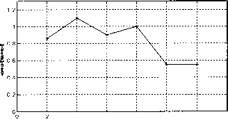 4 6 8 10 12 14 Nombre dharmoniques eliminees FIGURE 25.42 Evolution of the modulation index as a function of the number of harmonics eliminated.  FIGURE 25.43 by PSPICE. Simplified model of the switch with its antiparallel diode where
4. Solve (25.62) for da: da = - 5. Repeat 1 to 4 by correcting at each step by = a + da until the required precision is satisfied. Figure 25.42 shows the trajectory of the solutions for various values of R, with the modulation index MI varying in the interval [0 1.1] [31]. Figure 25.42a shows that there is a hnear progression of angles a and a2 following a negative or positive slope, respectively, in the interval 0 < MI < 0.6. This note is also valid for Fig. 25.42b; in Fig. 25.42c and 25.42d, however, in the interval 0.6 < MI < 1.1, these trajectories become nonlinear, and thus more refinement of the algorithm is carried out to obtain the solutions in this interval. As for Figs. 25.42e and 25.42f, the system has no solutions beyond MI > 0.6. We conclude from Fig. 25.42 that: Maximum of the modulation index diminishes with the increase of the harmonics number eliminated, illustrated in Fig. 25.43. For some values of R, the trajectories of the angles get nearer, which imphes a decrease in the width of pulses. 25.6.2 Simulation Results using PSPICE In order to check the validity of the calculated results of the angles, the three-phase inverter system connected to a load is modeled by using PSPICE [32]. The modehng of the switch is a simple version. It consists of an infinite value of resistance for the open state and a low-value resistance for the closed state. Figure 25.44 illustrates this principle. In order to model the inverter system of Fig. 25.40 We define: 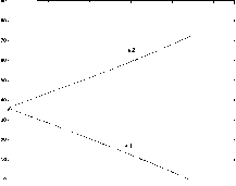 0.2 0.4 0.6 0.8 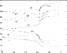 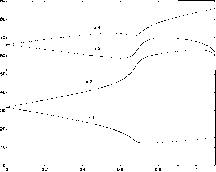   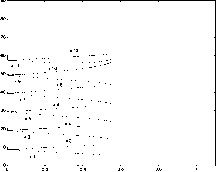 (c) if) FIGURE 25.44 Trajectories of solutions for programmed PWM: (a) К = 2ЛЪ) R = 4; (c) = 6; (d) = 8; (e) = 10; (f) = 12. by PSPICE, a simplified schematic diagram is adopted by 25.6.3 Simulated Results of the Programmed using the foUowing steps: PWM Control 1. Numbering the ties. 2. Components identification. PSPICE uses the circuit obtained to estabhsh a program. On the basis of the PSPICE program various simulations have been undertaken. Figure 25.45 iUustrates the results for the R = 2 and MI = 0.8, Fig. 25.45a represents the line case 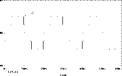 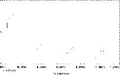 FIGURE 25.45 Simulation results for MI = 0.8 and R = 2: (a) Line voltage, (b) harmonics spectra; THD = 31.36%. FIGURE 25.48 Phasor diagram for leading and lagging mode. FIGURE 25.46 Main circuit of the ASVC. FIGURE 25.49 Equivalent circuit of the ASVC. FIGURE 25.47 Per-phase fundamental equivalent circuit. the calculation step beyond MI > 0.6 so as to obtain a finite solution. The increase in the harmonics number eliminated has a negative effect on the modulation index, since with the increase of a decrease in MI maximum follows. The trajectories getting nearer for MI > 0.6 implies a decrease in the switching pulses of the GTOs which itself allows for the increase in commutation losses. voltage and Fig. 25.45b its harmonic spectrum. We notice the total elimination of harmonics of order 5. 25.6.4 Conclusion The main conclusions are summarised as follows. The resolution of the nonlinear equations in the case of a three-level inverter must be carried out with a refinement of 25.7 Three-Level ASVC Structure Connected to the Network The fast-growing development of ultrarapid power switching devices and the desire to reduce the harmonics has led to an increase in the use of converters for large-scale reactive power compensation. Such an SVC is made up of two-level voltage source inverters and presents a fast response time and reduced 1 ... 59 60 61 62 63 64 65 ... 91 |
||||||||||||||||||||||||||||||||||||||||||||||||||||||||||||||||||||||||||||||||||||||||||||||
|
© 2026 AutoElektrix.ru
Частичное копирование материалов разрешено при условии активной ссылки |