 |
 |
 |
| Главная Журналы Популярное Audi - почему их так назвали? Как появилась марка Bmw? Откуда появился Lexus? Достижения и устремления Mercedes-Benz Первые модели Chevrolet Электромобиль Nissan Leaf |
Главная » Журналы » Metal oxide semiconductor 1 ... 4 5 6 7 8 9 10 ... 91 Power Bipolar Transistors Marcelo Godoy Simoes, Ph.D. Engineering Division Colorado School of Mines Golden, Colorado 80401-1887 USA 5.1 Introduction........................................................................................ 63 5.2 Basic Structure and Operation................................................................ 64 5.3 Static Characteristics............................................................................. 65 5.4 Dynamic Switching Characteristics.......................................................... 68 5.5 Transistor Base Drive Applications.......................................................... 69 5.6 Spice Simulation of Bipolar Junction Transistors....................................... 71 5.7 BJT Applications.................................................................................. 72 References........................................................................................... 74 5.1 Introduction The first transistor was created in 1948 by a team of physicists at the Bell Telephone Laboratories and soon became a semiconductor device of major importance. Before the transistor, amplification was achieved only with vacuum tubes. Although there are now integrated circuits with millions of transistors, flow and control of electrical energy still require single transistors. Therefore, power semiconductor switches constitute the heart of modern power electronics. Such devices should have larger voltage and current ratings, instant turn-on and turn-off characteristics, very low voltage drop when fully on, zero leakage current in blocking condition, enough ruggedness to switch highly inductive loads, which are measured in terms of safe operating area (SOA) and ES/b (reverse-biased second breakdown), high-temperature and radiation-withstand capabilities and high reliability. The right combination of such features restricts device suitability to only certain applications. Figure 5.1 depicts those voltage and current ranges, in terms of frequency, at which where the most common power semiconductors devices can operate. The figure actually gives an overall picture of where power semiconductors are typically applied in industries: High voltage and current ratings permit apphcations in large motor drives, induction heating, renewable energy inverters, FiVDC converters, and static VAR compensators and active filters. By contrast, low-voltage and high-frequency applications that include switching mode power supplies, resonant converters and motion control systems and low-frequency with high-current and voltage devices are restricted to cyclo-converter-fed and multimegawatt drives [1]. Power-npn or pnp bipolar transistors used to be the traditional components for driving several of these industrial applications. Fiowever, insulated-gate bipolar-transistor (IGBT) and metal-oxide-semiconductor field-effect transition (MOSFET) technology have progressed so much that they are now viable replacements for the bipolar types. Bipolar-npn or pnp transistors still have performance areas in which they still may be used; for example, they have lower saturation voltages over their operating temperature range, but they are considerably slower, exhibiting long turn-on and turn-off times. When a bipolar transistor is used in a totem-pole circuit, the most difficult design aspects to overcome are the base drive circuitry, i.e. the required circuit for driving the base. Although bipolar transistors have lower input capacitance than those of MOSFETs and IGBTs, they are current driven. Thus, the drive circuitry must generate high and prolonged input currents. The high input impedance of the IGBT is an advantage over its bipolar counterpart. Fiowever, input capacitance is also high. As a result, the drive circuitry must rapidly charge and discharge the input capacitor of the IGBT during the transition time. The IGBT low-saturation voltage performance is analogous to bipolar power-transistor performance, even over the operating-temperature range. The IGBT requires a -5/+ 10 V gate-emitter voltage transition to ensure reliable output switching. The MOSFET gate and IGBT are similar in many areas of operation. For instance, both devices have high input impedance, are voltage-driven, and use less silicon than the IMhz 1100 kHz I 10 kHz IkHz
2 kV 3 kV Voltage IMhz g 100 kHz 10 kHz IkHz Power MOSFET IGBT Thyristor 1kA 2 kA Current FIGURE 5.1 Power semiconductor operating regions, (a) voltage vs frequency; and (b) current vs frequency. bipolar power transistor to achieve the same drive performance. Additionally, the MOSFET gate has high input capacitance, which places the same requirements on the gate-drive circuitry as the IGBT employed at that stage. The IGBTs outperform MOSFETs when it comes to conduction loss vs supply-voltage rating. The saturation voltage of MOSFETs is considerably higher and less stable over temperature than that of IGBTs. For these reasons, the insulated-gate bipolar transistor took the place of bipolar junction transistors in several apphcations during the 1980s. Although the IGBT is a cross between the bipolar and MOSFET transistor, with the output switching and conduction characteristics of a bipolar transistor, but voltage-controlled like a MOSFET, the early IGBT versions were prone to latch up, which had been largely ehminated by the 1980s. Another characteristic with some IGBT types is the negative temperature coefficient, which can lead to thermal runaway and makes the paralleling of devices hard to achieve. Currently, this problem is being addressed in the latest generations of IGBTs. It is very clear that a categorization based on voltage and switching frequency provides two key parameters for determining whether a MOSFET or an IGBT is the better device in an application. However, there are still difficulties in selecting a component for use in the crossover region, which includes voltages of 250 to 1000 V and frequencies of 20 to 100 kHz. At voltages < 500 V, the BJT has been entirely replaced by MOSFET in power applications and has also been displaced at higher voltages, where new designs use IGBTs. Most regular industrial needs are in the range of 1-2 kV blocking voltages, 200-500 ampere conduction currents, and with switching speeds of 10-100 ns. Although in the last few years, new high voltage projects displaced BJTs towards IGBT, and it is expected that there will be a decline in the number of new power system designs that incorporate bipolar junction transistors, some applications for BJTs remain; in addition the huge built-up history of equipment installed in industries makes the bipolar junction transistor a good device. 5.2 Basic Structure and Operation The bipolar junction transistor (BJT) consists of a three-region structure of n-type and p-type semiconductor materials; it can be constructed as npn as well as pnp. Figure 5.2 shows the physical structure of a planar npn bipolar junction transistor. The operation is closely related to that of a junction diode where in normal conditions the pn junction between the base and collector is forward-biased (v > 0), causing electrons to be injected from the emitter into the base. As the base region is thin, the electrons travel across it and arrive at the reverse-biased base-collector junction (vq < 0), where there is an electric field (depletion region). Upon arrival at this junction the electrons are pulled across the depletion region and drawn into the collector. These electrons flow through the collector region and out the collector contact. Because electrons are negative carriers, their motion constitutes positive current flowing into the external collector terminal. Even though the forward-biased base-emitter junction injects holes from base to emitter, the holes do not contribute to the collector current but result in a net current flow component into the base from the external base terminal. Therefore, the emitter current is composed of these two components: electrons destined to be Forward-biased junction  Reverse-biased junction Collector FIGURE 5.2 Structure of a planar bipolar junction transistor. injected across the base-emitter junction, and holes injected from the base into the emitter. The emitter current is exponentially related to the base-emitter voltage by the equation: (5.1) where % is the saturation current of the base-emitter junction and which is a function of the doping levels, temperature and the area of the base-emitter junction, Vj is the thermal voltage Kt/q and rj is the emission coefficient. The electron current arriving at the collector junction can be expressed as a fraction a of the total current crossing the base-emitter junction tc = GCtE (5.2) Because the transistor is a three-terminals device, % is equal to ic + i, hence the base current can be expressed as the remaining fraction, % = (1 - (5.3) The collector and base currents are thus related by the ratio 1 -a (5.4) The values of a and for a given transistor depend primarily on the doping densities in the base, collector and emitter regions, as well as on the device geometry. Recombination and temperature also affect the values for both parameters. A power transistor requires a large blocking voltage in the off state and a high current capability in the on state; a vertically oriented four-layer structure as shown in Fig. 5.3 is preferable because it maximizes the cross-sectional area through which the current flows, enhancing the on-state Base Emitter  Collector figure 5.3 Power transistor vertical structure. Base Collector Base Emitter Emitter I Collector (a) (b) figure 5.4 Circuit symbols (a) NPN transistor; and (b) PNP transistor. resistance and power dissipation in the device [2]. There is an intermediate collector region with moderate doping, and the emitter region is controlled so as to have a homogeneous electrical field. Optimization of doping and base thickness are required to achieve high breakdown voltage and amplification capabilities. Power transistors have their emitters and bases interleaved to reduce parasitic ohmic resistance in the base current path, which also improves the device for second breakdown failure. The transistor is usually designed to maximize the emitter periphery per unit area of silicon, in order to achieve the highest current gain at a specific current level. In order to ensure those transistors have the greatest possible safety margin, they are designed to be able to dissipate substantial power and, thus, have low thermal resistance. It is for this reason, among others, that the chip area must be large and that the emitter periphery per unit area is sometimes not optimized. Most transistor manufacturers use aluminum metallization because it has many attractive advantages, among them easier application via vapor deposition and easier definition with photolithography. A major problem with aluminum is that only a thin layer can be applied by normal vapor-deposition techniques. Thus, when high currents are applied along the emitter fingers, a voltage drop occurs along them, and the injection efficiency on the portions of the periphery that are farthest from the emitter contact is reduced. This limits the amount of current each finger can conduct. If copper metallization is substituted for aluminum, then it is possible to lower the resistance from the emitter contact to the operating regions of the transistors (the emitter periphery). From a circuit point of view, Eqs. (5.1)-(5.4) are used to relate the variables of the BJT input port (formed by base (B) and emitter (E)) to the output port (collector (C) and emitter (E)). The circuit symbols are shown in Fig. 5.4. Most of power electronics apphcations use NPN transistors because electrons move faster than holes, and therefore, NPN transistors have considerable faster commutation times. 5.3 Static Characteristics Device static ratings determine the maximum allowable limits of current, voltage, and power dissipation. The absolute voltage limit mechanism is concerned with the avalanche in СЕ, sat
Increasing base current У Saturation region Constant-current (active) region (a) (b) figure 5.5 Family of current-voltage characteristic curves, (a) base-emitter input port; and (b) collector-emitter output port. terms of preventing thermal runaway. Forward current ratings are specified at which the junction temperature does not exceed a rated value so as to prevent leads and contacts from being evaporated. Power dissipated in a semiconductor device produces a temperature rise and is related to thermal resistance. A family of voltage-current characteristic curves is shown in Fig. 5.5. Figure 5.5a shows the base current % plotted as a function of the base-emitter voltage v and Fig. 5.5b depicts the collector current as a function of the collector-emitter voltage Ve ith as the controlling variable. Figure 5.5 shows several curves distinguished from each other by the value of the base current. The active region is defined where flat, horizontal portions of voltage-current curves show constant current, because the collector current does not change significantly with Vq for a given Those portions are used only for small signal transistors operating as linear amphfiers. On the other hand, switching power electronics systems require transistors to operate in either the saturation region where Vq is small or in the cutoff region where the current is zero and the voltage is upheld by the device. A small base current drives the flow of a much larger current between collector and emitter; such gain (called beta - Eq. (5.4)) depends upon temperature, Ve c-Figure 5.6 shows current gain increase with increased collector voltage; gain falls off at both high and low current levels. High voltage BJTs typically have low current gain, and hence Darlington-connected devices, as indicated in Fig. 5.7 are commonly used. Considering gains and P2 one of these transistors, the Darhngton connection will have an increased gain of + 2 + iii2 diode Dl speeds up the turn-off process by allowing the base driver to remove the stored charge on the transistor bases. О и vee = 2V(125 °С)  = 400 V (25 °С) log(ic) figure 5.6 Current gain depends on temperature Fe and 7. Vertical-Structure power transistors have an additional region of operation called quasi-saturation, indicated in the characteristics curve of Fig. 5.8. Such a feature is a consequence of the lightly doped collector drift region where the collector base junction supports a low reverse bias. If the transistor enters the hard-saturation region the on-state power dissipation is minimized; there is, however, a tradeoff- in quasi-saturation the stored charges are smaller. At high D, 1 figure 5.7 Darlington-connected BJTs. / quasi-saturation breakdown 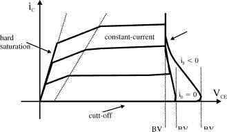 ic limit P,o,limit SUS * CEO * CBO FIGURE 5.8 Voltage-current characteristics for a vertical power transistor. collector currents beta gain decreases with increased temperature and with quasi-saturation operation such negative feedback allows careful device paralleling. Two mechanisms at the microelectronic level determine the fall-off in beta, namely conductivity modulation and emitter crowding. One can note that there is a region called primary breakdown due to conventional avalanche of the C-B junction and the attendant large flow of current. Fiere VguS the limit for primary breakdown, is the maximum collector-emitter voltage that can be sustained across the transistor when it is carrying high collector current. The Vgus lower than Veo свс both of which measure the transistors voltage standoff capability when the base current is zero or negative. The bipolar transistor has another potential failure mode called second breakdown, which shows as a precipitous drop in the collector-emitter voltage at large currents. Because the power dissipation is not uniformly spread over the device but is, instead, rather concentrated on regions, this serves to make the local gradient of temperature rise very quickly. Such thermal runaway brings hot spots that can eventually melt and recrys-tallize the silicon, thereby resulting in device destruction. The key to avoiding second breakdown is to: (1) keep power dissipation under control; (2) use a controlled rate of change of base current during turn-off; (3) use protective snubber circuitry; and (4) position the switching trajectory within the safe operating area (SOA) boundaries. In order to describe the maximum values of current and voltage to which the BJT should be subjected, two diagrams are used: the forward-bias safe operating area (FBSOA) given in Fig. 5.9 and the reverse-bias safe operating area (RBSOA) shown in Fig. 5.10. In the FBSOA current /q is the maximum current of the device and there is a boundary defining the maximum thermal dissipation and a margin defining the second breakdown hmitation. These regions are expanded for switching mode operation. Inductive load generates a higher peak energy at turn-off than does its resistive counter- Pulsed-SOA Secondary /breakdown  FIGURE 5.9 Forward-bias safe operating area (FBSOA). part. It is then possible to have a secondary breakdown failure if RBSOA is exceeded. A reverse base current helps the internal operation leading to an expanded region RBSOA. The RBSOA curve shows that for voltages below У^ео the safe area is independent of reverse bias voltage Уев is only limited by the device collector current, whereas above Veo the collector current must be under control, dependent upon the apphed reverse-bias voltage; in addition, temperature effects derate the safe operating area. The ability of a transistor to switch high currents reliably is thus determined by its peak power-handling capabilities. This ability is dependent upon both the transistors current and thermal density throughout the active region. In order to optimize the safe operating area (SOA) capability, both current- and thermal density must be low. In general, it is the hot spots occurring at the weakest area of the transistor that will cause a device to fail due to second breakdown phenomena. Although a wide base width will hmit the current density across the base region, good heat sinking directly under the collector will enable the transistor to withstand high peak power. When the power and heat are spread over a large silicon area, all of these destructive tendencies are held to a minimum, and the transistor will have the highest SOA capability. When the transistor is on, one can ignore the base current losses and calculate power dissipation on the on state (conduction losses) with Eq. (5.5). Fiard saturation minimizes collector-emitter vohage, which decreases on-state losses. (5.5)
FIGURE 5.10 Reverse-bias safe operating area (RBSOA). 5.4 Dynamic Switching Characteristics Switching characteristics are important in defining device velocity during change fi-om conduction (on) to blocking (off) states. Such transition velocity is of paramount importance because most of the losses are due to high frequency switching. Figure 5.11 shows typical waveforms for a resistive load. Index r refers to the rising time (from 10 to 90% of maximum value); for example t is the current rise time and depends upon base current. The falhng time is indexed by / ; the parameter % is the current falling time, that is, when the transistor is blocking such time corresponds to crossing from the saturation to the cutoff state. In order to improve %, the base current for blocking must be negative and the device must be kept in quasi-saturation so as to minimize stored charges. The delay time is denoted by corresponding to the time to discharge the capacitance of junction base-emitter, which time can be reduced with a larger current base with high slope. Storage time (tJ is a very important parameter for BJT transistors, it is the time required to neutralize the carriers stored in the collector and the base. Storage time and switching losses are key points when dealing with bipolar power transistors. Switching losses occur at both turn-on and turn-off. For high-frequency operation the rising and falling times for voltage and current transitions play an important role as indicated by Fig. 5.12. A typical inductive load transition is indicated in Fig. 5.13. The figure indicates a turn-off transition. Current and voltage are interchanged at turn-on and an approximation based upon straight line switching intervals (resistive load) gives the switching losses calculated using Eq. (5.6). P -Tf (5.6)  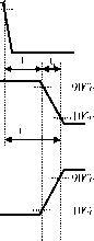 Base current Collector current Voltage Vc] о о и о > JrfL. Switching losses Conduction losses FIGURE 5.12 Inductive load switching characteristics. where т is the duration of the switching interval and and 1 are the maximum voltage and current levels as shown in Fig. 5.14. Most advantageous operation is achieved when fast transitions are optimized. Such a requirement minimizes switching losses. Therefore, a good bipolar drive circuit influences significantly the transistor performance. A base drive circuit should provide a high forward base drive current (J) as indicated in Fig. 5.14 if power semiconductor turn-on is to be ensured quickly. Base drive current should keep the BJT fully saturated so as to minimize forward conduction losses, but a level 12 would maintain the transistor in quasi-saturation, which avoids an excess of charges in the base. Controllable Voltage, Current Voltage, Current  FIGURE 5.11 Resistive load dynamic response. FIGURE 5.13 Turn-off voltage and current switching transition, (a) inductive load; and (b) resistive load.  \/ dt FIGURE 5.14 Recommended base current for BJT driving. slope and reverse current 4 sweep out stored charges in the transistor base, speeding up device turn-off. 5.5 Transistor Base Drive Applications A plethora of circuits has been suggested to command transistors successfully for operation in power electronics switching systems [3]. Such base drive circuits try to satisfy the following requirements: supply the right collector current; adapt the base current to the collector current; and extract a reverse current from base to speed up device blocking. A good base driver reduces the commutation times and total losses, thus increasing efficiency and operating frequency. Depending upon the grounding requirements between the control and the power circuits, the base drive might be either an isolated or nonisolated type. Figure 5.15 shows a nonisolated circuit. When is switched on, T2 is driven and diode is forward-biased, which provides a reverse bias and keeps T3 off. The base current 1 is positive and saturates the power transistor Tp. When is switched off, T3 switches on due to the negative path provided by and -VCC, providing a negative current for switching off the power transistor Tp. When a negative power supply is not provided for the base drive, a simple circuit like Fig. 5.16 can be used in low-power apphcations (stepper motors, small dc-dc converters, relays, pulsed circuits). When the input signal is high switches on   FIGURE 5.16 Base command without negative power supply. and a positive current goes to Tp, thus keeping the capacitor charged with the Zener voltage; and when the input signal falls, T2 provides a path for the discharge of the capacitor, which imposes a pulsed negative current from the base-emitter junction of Tp. A combination of large reverse base drive and antisaturation techniques may be used to reduce storage time to almost zero. A circuit called Bakers clamp may be employed as illustrated in Fig. 5.17. When the transistor is on its base it is two diode drops below the input. Assuming that diodes D2 and D3 have a forward bias voltage of 0.7 V, then the base will be 1.4 V below the input terminal. Due to diode the collector is one diode drop, or 0.7 V below the input. Therefore, the collector will always be more positive than the base by 0.7 V, staying out of saturation; further because collector voltage increases the gain also increases slightly. Diode D4 provides a negative path for the reverse base current. The input base current can be supplied by a driver circuit similar to the one discussed in Fig. 5.15. Several situations require ground isolation, off-line operation, and floating transistor topology. In addition, safety needs may require an isolated base drive circuit. Numerous circuits have been demonstrated in switching power supplies to isolated topologies, usually integrating base drive requirements with their power transformers. Isolated base drive D2 D3 FIGURE 5.15 Nonisolated base driver. FIGURE 5.17 Antisaturation diodes (Baker clamps) improve power transistor storage time.   FIGURE 5.18 Isolated base drive circuit. FIGURE 5.20 Proportional base drive circuit. circuits may provide either constant current or proportional current excitation. A very popular base drive circuit for floating switching transistor is shown in Fig. 5.18. When a positive voltage is impressed on the secondary winding (V) of Tji, a positive current flows into the base of the power transistor Tp and it switches on (resistor hmits the base current). Capacitor is charged by (- Vp, - V) and is kept blocked because diode reverse biases the base-emitter. When V5 is zipped off, the capacitor voltage Vq brings the emitter of to a negative potential in respect to its base. Therefore, is excited so as to switch on and start pulling a reverse current from the Tp base. Another very effective circuit is shown in Fig. 5.19 with a minimum number of components. The base transformer has a tertiary winding, which uses the energy stored in the transformer to generate the reverse base current during the turn-off command. Other configurations are also possible by adding to the isolated circuits the Baker clamp diodes, or Zener diodes with paralleled capacitors. Sophisticated isolated base drive circuits can be used to provide proportional base drive currents where it is possible to control the value of P; by keeping it constant for all collector currents shorter storage time results. Figure 5.20 shows one possible way to realize a proportional base drive circuit. When  FIGURE 5.19 transformer. Transformer coupled base drive with tertiary winding transistor Tl turns on, the transformer Tpi is in negative saturation and power transistor Tp is off. During the time that Tl is on a current flows through winding iV, limited by resistor Rl, storing energy in the transformer and holding it at saturation. When transistor turns off, the energy stored in N1 is transferred to winding N4, pulling the core from negative to positive saturation. Windings N2 and N4 will withstand as a current source, transistor Tp will stay on, and gain will be imposed by the turns ratio given by: (5.7) To use the proportional drive given in Fig. 5.20 careful design of the transformer must be done in order to have the flux balanced, which will then keep the core under saturation. Transistor gain must be somewhat higher than the value imposed by the transformer turns ratio, which requires cautious device matching. The most critical portion of the switching cycle occurs during transistor turn-off because normally reverse-base current is made very large in order to minimize storage time and such a condition may avalanche the base-emitter junction and lead to destruction. There are two options to prevent this from happening: turning off the transistor at low values of collector-emitter voltage (which is not practical in most of the apphcations), or reducing collector current with rising collector voltage, implemented by RC protective networks called snubbers. Therefore, an RC snubber network can be used to divert the collector current during the turn-off, which then improves the reverse bias safe operating area; in addition, the snubber circuit dissipates a fair amount of switching power and this reheves the transistor. Figure 5.21 shows a turn-off snubber network; when the power transistor is off capacitor С is charged through diode Dl. Such collector current flows temporarily into the capacitor as the collector-voltage rises; as the power transistor turns on, the capacitor discharges through the resistor R back into the transistor.  FIGURE 5.21 Turn-off snubber network. It is not possible to fully develop all aspects of simulation of BJT circuits. Before giving an example, some comments are necessary regarding modeling and simulation of bipolar junction transistor circuits. There are several types of commercial circuit simulation programs available on the market, extending from a set of functional elements (passive components, voltage controlled and current sources, semiconductors) which can be used to model devices, to other programs that have the possibility of implementing algorithm relationships. Those streams are called subcircuit (building auxiliary circuits around a SPICE primitive) and mathematical (deriving models from internal device physics) methods. Simulators can solve circuit equations exactly, giving models for the nonlinear transistors, and predict the analog behavior of the node voltages and currents in continuous time. They are costly in computer time and such programs have not been written normally to serve the needs of power electronic circuit design but rather they are used to design low-power and low-voltage electronic circuits. Therefore, one has to decide which approach should be taken for incorporating BJT power transistor modeling, and a trade-off between accuracy and simplicity must be considered. If precise transistor modeling is required, subcircuit-oriented programs should be used. On the other hand, when simulation of complex power electronic system structures or novel power electronic topologies are devised, switch modeling should be rather simple, (which can be accomplished by taking into consideration fundamental switching operations) and a mathematically oriented simulation program should be used. 5.6 SPICE Simulation of Bipolar Junction Transistors A general-purpose circuit program that can be apphed to simulate electronic and electrical circuits and predict circuit behavior, SPICE was originally developed at the Electronics Research Laboratory of the University of California, Berkeley (1975). The name stands for simulation program for inte- grated circuits emphasis. A circuit must be specified in terms of element names, element values, nodes, variable parameters, and sources. Several types of circuit analysis are possible using SPICE: nonhnear dc analysis - calculates dc transference; nonhnear transient analysis - calculates signals as a function of time; hnear ac analysis - computes a Bode plot of output as a function of frequency; noise analysis; sensitivity analysis; distortion analysis; Fourier analysis; and Monte-Carlo analysis. PSpice is a commercial version which has analog and digital libraries of standard components such as operational amph-fiers, digital gates, and flip-flops. This makes it a useful tool for a wide range of analog and digital apphcations. An input file, called source file, consists of three parts: (1) data statements, with description of the components and the interconnections; (2) control statements, which tell SPICE what type of analysis to perform on the circuit; and (3) output statements, with specifications of which outputs are to be printed or plotted. Two other statements are required - the title statement and the end statement. The title statement is the first line and can contain any information, while the end statement is always .END. This statement must be a line by itself, followed by carriage return. In addition, there are also comment statements, which must begin with an aterisk and are ignored by SPICE. There are several model equations for bipolar junction transistors. The SPICE system has built-in models for semiconductor devices, and the user only needs to specify the pertinent model parameter values. The model for the BJT is based on the integral-charge model of Gummel and Poon [4]. Fiowever, if the Gummel-Poon parameters are not specified, the model reduces to the piecewise-linear Ebers-MoU model as depicted in Fig. 5.22. In either case, charge-storage effects, ohmic resistances, and a current-dependent output conductance may be included. The forward gain characteristics are defined by the parameters IS and BF, the reverse characteristics by IS and BR. Three ohmic resistances RB, RC, and RE are also included. The two diodes are modelled by voltage sources and experimental Shockley equations can be transformed into logarithmic ones. A set of device model parameters is defined on a separate MODEL card and assigned a unique model name. The device element cards in SPICe then reference the model name. This scheme lessens the need to specify all of the model parameters on each device element card. Parameter values are defined by appending the parameter name, as given here for each model type, followed by an equal sign and the parameter value. Model parameters not given a value are assigned the default values given here for each model type. Collector Base Rfl  Emitter FIGURE 5.22 Ebers-MoU transistor model. As an example, the model parameters for the 2N2222A NPN transistor are given in what follows: .MODEL Q2N222A NPN (IS=14.34F XTI=3 EG=1.11 VAF=74.03 BF=255.9 NE=1.307 ISE=14.34F IKF=.2847 XTB=1.5 BR=6.092 N0=2 ISO=0 IKR=0 RC=1 OJO=7.306P MJO=.3416 VJO=.75 F0=.5 OJE=22.01P MJE=.377 VJE=.75 TR=46.91N TF=4.11.1P ITF=.6 VTF=1.7 XTF=3 RB=10) Figure 5.23 shows a BJT buck chopper. The dc input voltage is 12 V, load resistance R is 5 Q, filter inductance L is 145.8 iH and the filter capacitance С is 200 iF. The chopping frequency is 25 kHz and the duty cycle of the chopper is 42% as indicated 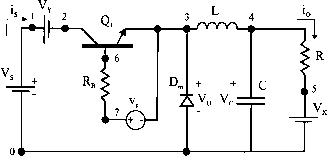 FIGURE 5.23 BJT buck chopper. by the control voltage statement (Vq). The listing that follows plots the instantaneous load current (/q), the input current (/5), the diode voltage (V), the output voltage (Vq) and calculates the Fourier coefficients of the input current (/5). This listing for the careful reader as it provides more details and enhancements that are useful when SPICE is chosen for simulations as shown below. 5.7 BJT Applications Bipolar junction power transistors are applied to a variety of power electronic functions, switching mode power supplies, dc motor inverters, PWM inverters [5], and many other functions too numerous to name. To conclude, three applications are illustrated. A flyback converter is given in Fig. 5.24. The switching transistor is required to withstand peak collector voltage at turn-off and peak collector currents at turn-on. In order to limit the collector voltage to a safe value, the duty cycle must
1 ... 4 5 6 7 8 9 10 ... 91 |
|||||||||||||||||||||||||||||||||||||||||||||||||||||||||||||||||||||||||||||||||||||||||||||||||||||||||||||||||||||||||||||||||||||||||||||
|
© 2026 AutoElektrix.ru
Частичное копирование материалов разрешено при условии активной ссылки |