 |
 |
 |
| Главная Журналы Популярное Audi - почему их так назвали? Как появилась марка Bmw? Откуда появился Lexus? Достижения и устремления Mercedes-Benz Первые модели Chevrolet Электромобиль Nissan Leaf |
Главная » Журналы » Metal oxide semiconductor 1 ... 5 6 7 8 9 10 11 ... 91 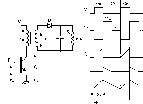 ---- )UT T -► FIGURE 5.24 Flyback converter. be kept relatively low, normally <50%, that is, д < 0.5. In practice, the duty-cycle is taken at 0.4, which hmits the peak collector. A second design factor the transistor must meet is the working collector current at turn-on, dependent on the primary transformer-choke peak current, the primary-to- secondary turns ratio, and the output load current. When the transistor turns on, the primary current builds up in the primary winding and thus stores energy, as the transistor turns off, the diode at the secondary winding is forward biasing, which releases the stored energy into the output capacitor and 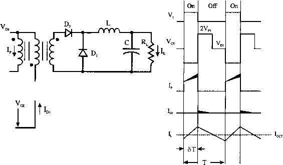 /1 ii- FIGURE 5.25 Isolated forward converter.  FIGURE 5.26 Chopper-fed dc drive. load. Such a transformer operating as a coupled inductor is actually defined as a transformer-choke. The transformer-choke of the flyback converter must be designed carefully so as to avoid saturation because the operation is unidirectional on the B-H characteristic curve. Therefore, a core with a relatively large volume and air gap must be used. An advantage of the flyback circuit is the simplicity by which a multiple output switching power supply may be realized. This is because the isolation element acts as a common choke to all outputs and thus only a diode and a capacitor are needed for an extra output voltage. Figure 5.25 shows the basic forward converter and its associated waveforms. The isolation element in the forward converter is a pure transformer that should not store energy and, therefore, a second inductive element L is required at the output for proper and efficient energy transfer. Notice that the primary and secondary windings of the transformer have the same polarity, that is, the dots are at the same winding ends. When the transistor turns on, current builds up in the primary winding. Because of the same polarity of the transformer secondary winding, such energy is forward transferred to the output and also stores in inductor L through diode D2, which is forward-biased. When the transistor turns off, the transformer winding voltage reverses, back-biasing diode D2, and the flywheel diode D3 is forward-biased, conducting currents in the output loop and delivering energy to the load through inductor L The tertiary winding and diode D provide transformer demagnetisation by returning the transformer magnetic energy into the output dc bus. It should be noted that the duty cycle of the switch b must be kept < 50% so that when the transformer voltage is clamped through the tertiary winding, the integral of the volt-seconds between the input voltage and the clamping level balances to zero. Duty cycles >50%, that is, д > 0.5, will upset the volt-seconds balance, driving the transformer into saturation, which in turn produces high collector current spikes that may destroy the switching transistor. Although the clamping action of the tertiary winding and the diode limit the transistor peak collector voltage to the dc input, care must be taken during construction to couple the tertiary winding tightly to the primary (bifilar wound) to ehminate voltage spikes caused by leakage inductance. Chopper drives are connected between a fixed-voltage dc source and a dc motor to vary the armature voltage. In addition to armature voltage control, a dc chopper can provide regenerative braking of the motors and will return energy back to the supply. This energy-saving feature is desirable for transportation systems such as mass rapid transit ones (MRT) and chopper drives are also used in battery electric vehicles. A dc motor can be operated in one of the four quadrants by controlling the armature of field voltages (or currents). It is often required that the armature or field terminals be reversed in order to operate the motor in the desired quadrant. Figure 5.26 shows a circuit arrangement of a chopper-fed dc separately excited motor. This is a one-quadrant drive and the waveforms for the armature voltage, load current, and input current are also shown. By varying the duty cycle, the power flow to the motor (and speed) can be controlled. References 1. Bimal K. Bose, Power Electronics and Ac Drives, Prentice-Hall, Engle-wood Cliffs, NJ, 1986. 2. Ned Mohan, Tore M. Underland, and William P. Robbins, Power Electronics: Converters, Applications, and Design, John Wiley & Sons, NY, 1995. 3. George C. Chryssis, High Frequency Switching Power Supplies: Theory and Design, McGraw-Hill, NY, 1984. 4. Muhammad H. Rashid, Power Electronics: Circuits, Devices, and Applications, Prentice-Hall, Englewood Cliffs, NH, 1993. 5. B. W. Williams, Power Electronics: Devices, Drivers and Applications, John Wiley & Sons, NY, 1987. The Power MOSFET Issa Batarseh College of Engineering and Computer Science University of Central Florida Orlando, Florida 32816, USA batarseh@mail. ucf. edu 6.1 6.2 6.3 6.4 6.5 6.8 6.9 Introduction........................................................................................ 75 The Need for Switching in Power Electronic Circuits................................. 76 General Switching Characteristics............................................................ 78 6.3.1 The Ideal Switch 6.3.2 The Practical Switch The Power MOSFET............................................................................. 80 MOSFET Structure............................................................................... 81 6.5.1 On-state Resistance 6.5.2 Internal Body Diode 6.5.3 Internal Capacitors MOSFET Regions of Operation.............................................................. 83 6.6.1 MOSFET Switching Characteristics 6.6.2 Turn-on Characteristics 6.6.3 Turn-off Characteristics 6.6.4 Safe-Operation Area MOSFET PSpice Model......................................................................... 93 6.7.1 Static Model 6.7.2 Large Signal Model Comparison of Switching Devices........................................................... 96 Future Trends in Power Devices.............................................................. 98 References........................................................................................... 99 6.1 Introduction This chapter gives an overview of power MOSFET semiconductor switching devices. Detailed discussion of the physical structure, fabrication and physical behavior of the device and packaging is beyond the scope of this chapter. The emphasis here will be on the terminal i-v switching characteristics of the available device, turn-on and turn-off switching characteristics, PSpice modeling and its current voltage and switching limits. Even though, most of todays available semiconductor power devices are made of silicon or germanium materials, other materials such as gallium arsenide, diamond and sihcon carbide are currently being tested. One of the main contributions that led to the growth of the power electronics field has been the unprecedented advancement in semiconductor technology, especially with respect to switching speed and power handling capabilities. The area of power electronics started by the introduction of the sihcon controlled rectifier (SCR) in 1958. Since then, the field has grown in parallel with the growth of the power semiconductor device technology. In fact, the history of power electronics is very much connected to the development of switching devices and it emerged as a separate disciphne when high-power and MOSFET devices were introduced in the 1960s and 1970s. Since then, the introduction of new devices has been accompanied by dramatic improvement in power rating and switching performance. Because of their functional importance. drive complexity, fragility, and cost, the power electronic design engineer must be equipped with a thorough understanding of the device operation, hmitation, drawbacks, and related reliability and efficiency issues. In the 1980s, the development of power semiconductor devices took an important turn when new process technology was developed that allowed integration of MOS and bipolar junction transistor (BJT) technologies on the same chip. Thus far, two devices using this new technology have been introduced: insulated bipolar transition (IGBT) and MOS-controUed thyristor (MCT). Many integrated circuit (1С) processing methods as well as equipment have been adapted for the development of power devices. Fiowever, unlike microelectronic ICs, which process information, power device ICs process power and so their packaging and processing techniques are quite different. Power semiconductor devices represent the heart of modern power electronics, with two major desirable characteristics of power semiconductor devices guiding their development: 1. switching speed (turn-on and turn-off times); and 2. power handling capabilities (voltage blocking and current carrying capabilities). Improvements in both semiconductor processing technology and manufacturing and packaging techniques have allowed power semiconductor development for high-voltage and high current ratings and fast turn-on and turn-off characteristics. Today, switching devices are manufactured with amazing power handhng capabihties and switching speeds as will be shown later. The availability of different devices with different switching speeds, power handling capabilities, size, cost etc., makes it possible to cover many power electronics applications. As a result, trade-offs are made when it comes to selecting power devices. 6.2 The Need for Switching in Power Electronic Circuits As already stated, the heart of any power electronic circuit is its semiconductor-switching network. The question arises here as to whether we have to use switches to perform electrical power conversion from the source to the load. The answer, of course, is no, as there are many circuits that can perform energy conversion without switches, including linear regulators and power amplifiers. However, the need to use semiconductor devices to perform conversion functions is very much related to converter efficiency. In power electronic circuits, the semiconductor devices are generally operated as switches, that is, either in the on-state or the off-state. This is unhke the case for power amphfiers and linear regulators where semiconductor devices operate in the hnear mode. As a result, a very large amount of energy is lost within the power circuit before the processed energy reaches the output. Semiconductor switching devices are used in power electronic circuits because of their ability to control and manipulate very large amounts of power from the input to the output with a relatively very low power dissipation in the switching device. Their use helps to create a very highly efficient power electronic system. Efficiency is considered an important figure of merit and has significant implications for overall system performance. Low efficiency power systems, large amounts of power are dissipated in the form of heat, which results in one or more of the following imphcations: 1. Cost of energy increases due to increased consumption. 2. Additional design complications might be imposed, especially regarding the design of device heat sinks. 3. Additional components such as heat sinks increase cost, size and weight of the system, resulting in low-power density. 4. High-power dissipation forces the switch to operate at low switching frequency, resulting in hmited bandwidth, slow response, and most important, the size and weight of magnetic components (inductors and transformers) and capacitors remain large. Therefore, it is always desired to operate switches at very high frequencies. However, we will show later that as the switching frequency increases, the average switching power dissipation increases. Hence, a trade-off must be made between reduced size, weight and cost of components versus reduced switching power dissipation, which means inexpensive low switching frequency devices. 5. Reduced component and device rehability. For more than 30 years, it has been shown that switching (mechanical or electrical) is the best possible way to achieve high efficiency. However, unlike mechanical switches, electronic switches are far more superior because of their speed and power handling capabilities as well as reliability. We should note that the advantages of using switches do not come without a cost. Because of the nature of switch currents and voltages (square waveforms), high-order harmonics are normally generated in the system. To reduce these harmonics, additional input and output filters are normally added to the system. Moreover, depending on the device type and power electronic circuit topology used, driver circuit control and circuit protection can significantly increase both the complexity of the system and its cost. Example 6.1. The purpose of this example is to investigate the efficiency of four different power circuits whose functions are to take in power from 24-V dc source and deliver a 12-V dc output to a 6-Q resistive load. In other words, these circuits serve as a dc transformer with a ratio of 2:1. The four circuits shown in Fig. 6.1a,b,c,d represent the voltage divider circuit, Zener regulator, transistor linear regulator, and switching circuit, respectively. The objective is to calculate the efficiency of these four power electronic circuits. Solution 6.1. Voltage divider dc regulator: The first circuit, the simplest, forms a voltage divider with R = R = eQ. and = 12 V. The efficiency defined as the ratio of the average load power to the average input power, P Rp + R In fact, efficiency is simply V,/V %. As the output voltage becomes smaller, the efficiency decreases proportionally. Zener dc Regulator: Since the desired output is 12 V, we select a Zener diode with Zener breakdown = 12 V. Assume the Zener diode has the i-v characteristic shown in Fig. 6.1(e); as ij = 6 Q, the load current 4, is 2 A. Then we calculate R for 1 = 0.2 A (10% of the load current). This results in = 5.27 Q. The input power is Pin = 2.2 A X 24 V = 52.8 W and the output power is -A/W б  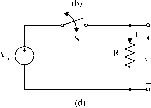
switch   0 DT FIGURE 6.1 (a) Voltage divider; (b) Zener regulator; (c) transistor regulator; (d) switching circuit; (e) i-v Zener diode characteristics and (f) switching and output waveforms. P = 24 W. The efficiency of the circuit is given by 24 W 52.8 W = 45.5% Transistor dc Regulator: It is clear from Fig. 6.1c that for = 12 V, the collector emitter voltage must by 12 V. Fience, the control circuit must provide base current to put the transistor in the active mode with Ve 12 V. As the load current is 2 A, then collector current is approximately 2 A (assume small 1). The total power dissipated in the transistor can be approximated by the following equation: diss = cec + Be4 12 X 2 = 24 W Therefore, the efficiency of the circuit is 50%. Switching dc Regulator: Let us consider the switching circuit of Fig. 6. Id by assuming the switch is ideal and is periodically turned on and off in Fig. 6. If. The output voltage waveform is shown in Fig. 6.If. Although the output voltage is not constant or pure dc, its average value is given by V =i o,ave Y where D is the duty ratio and it equals the ratio of the on-time to the switching period. For ave = 12 V, we set D = 0.5, that is, the switch has a duty cycle of 0.5 or 50%. Fiere the average output power is 48 W and the average input power is also 48 W, resulting in 100% efficiency! This is of course because we assumed that the switch is ideal. Fiowever, if we assume that a BJT switch is used in forementioned circuit with VEsat = 1 V and is small, then the average power loss across the switch is approximately 2 W, which creates an overall efficiency of 96%. Of course, the switching circuit given in this example is over simplified because the switch requires additional driving circuitry that was not shown, and which also dissipates some of the power. Fiowever, the example illustrates that higher efficiency can be obtained by switching to a power electronic circuit as compared to the efficiency obtained from a hnear power electronic circuit. Further, the difference between the linear circuit in Fig. 6.1b and 6.1c and the switched circuit of Fig. 6. Id is that the power delivered to the load in the latter case pulsates between zero and 96 W. If the application calls for constant power delivery with little output voltage ripple, then an LC filter must be added to smooth out the output voltage. A final observation is required on what is known as load and line regulation. Line regulation is defined as the ratio between the change in output vohage AV, with respect to the change in the input vohage AVin- These are very important parameters in power electronics because the dc input voltage is obtained from a rectified hne voltage that normally changes by ±20%. Therefore, any off-line power electronics circuit must have a hmited or specified range of line regulation. If we assume that the input voltage in Fig. 6.1a,b is changed by 2 V, that is AV = 2 V, and with unchanged, the corresponding change in the output voltage AV is IV and 0.55 V, respectively. This is considered very poor hne regulation. Figure 6.1c,d have much better line and load regulations because the closed-loop control compensates for the line and load variations. 6.3 General Switching Characteristics 6.3.1 The Ideal Switch It is always desirable to have power switches perform as close as possible to the ideal case. For a semiconductor device to operate as an ideal switch, it must possess the foUowing features: 1. no hmit on the amount of current (known as forward or reverse current) the device can carry when in the conduction state (on-state); 2. No limit on the amount of device-voltage ((known as forward- or reverse-blocking voltage) when the device is in the nonconduction state - off-state; 3. zero on-state voltage drop when in the conduction state; 4. infinite off-state resistance, that is, zero leakage current when in the nonconduction state; and 5. no limit on the operating speed of the device when a state is changed, that is, zero rise and faU times. The switching waveforms for an ideal switch are shown in Fig. 6.2, where 4w sw e the current through and the voltage across the switch, respectively. During switching and conduction periods the power loss is zero, resulting in a 100% efficiency; with no switching delays, an infinite operating frequency can be achieved. In short, an ideal switch has infinite speed, unlimited power handling capabilities, and 100% efficiency. It must be noted that it is not surprising to find semiconductor-switching devices that for aU practical purposes can almost perform as ideal switches for number of applications. 6.3.2 The Practical Switch The practical switch has the foUowing switching and conduction characteristics: 1. Limited power handling capabilities, that is, limited conduction current when the switch is in the on-state.  pit) FIGURE 6.2 Ideal switching current, voltage and power waveforms. and limited blocking voltage when the switch is in the off-state. 2. Limited switching speed caused by the finite turn-on and turn-off times. This limits the maximum operating frequency of the device. 3. Finite on-state and off-state resistances, that is, forward voltage drop exists when in the on-state, and reverse current flow (leakage) exists when in the off-state. 4. Because of characteristics 2 and 3, the practical switch experiences power losses in the on- and off-states (known as conduction loss), and during switching transitions (known as switching loss). The typical switching waveforms of a practical switch are shown in Fig. 6.3a. The average switching power and conduction power losses can be evaluated from these waveforms. We should point out that the exact practical switching waveforms vary from one device to another device, but Fig. 6.3a gives a reasonably good representation. Moreover, other issues such as temperature dependence, power gain, surge capacity, and over-voltage capacity must be considered when addressing specific devices for specific apphcations. A useful plot that illustrates how switching takes place from on to off and vice versa is what is called switching trajectory, which is simply a plot of 4w s v. Forward voltage drop 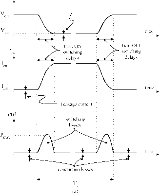 Typical practical waveform \ ON OFF (Highly Inductive load) 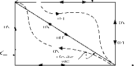 (Ideal Switch) pOFPr ON OFF FIGURE 6.3 (a) Practical switching current, voltage and power waveforms; and (b) switching trajectory. Figure 3(b) shows several switching trajectories for the ideal and practical cases under resistive loads. Example 6.2. Consider a linear approximation of Fig. 6.3a as shown in Fig. 6.4a: (a) give a possible circuit implementation using a power switch whose switching waveforms are shown in Fig. 6.4a; (b) derive the expressions for the instantaneous switching and conduction power losses and sketch them; (c) determine the total average power dissipated in the circuit during one switching frequency; and (d) determine the maximum power. Solution 6.2. (a) First let us assume that the turn-on time ton and turn-off time tff, the conduction voltage Vqn the leakage current /qff e part of the switching characteristics of the switching device and have nothing to do with circuit topology. When the switch is off, the blocking voltage across the switch is Vqff which can be represented as a dc voltage source of value Vqff reflected somehow across the switch during the off-state. When the switch is on, the current through the switch equals /qn id hence a dc current is needed in series with the switch when it is in the on-state. This suggests that when the switch turns off again, the current in series with the switch must be diverted somewhere else (this process is known as 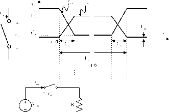
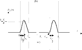 FIGURE 6.4 Linear approximation of typical current and voltage switching waveforms. commutation). As a result, a second switch is needed to carry the main current from the switch being investigated when it is switched off. However, as 4w sw hnearly related as shown in Fig. 6.4, a resistor will do the trick and a second switch is not needed. Figure 6.4 shows a one-switch implementation with S the switch and R the switched-load. (b) The instantaneous current and voltage waveforms during the transition and conduction times are given as foUows: 4w(0 = (ON ~ 4)Ff) + k 0 < t < toN toff (ON ~ OFf) + OFF - foFF <t<Z (t - on) + ( off - on 0 < t < on s ~ ff (t - (T, - toFF)) + on Ts - toFF <t<T, It can be shown that if we assume /qn > off OFF V, then the instantaneous power = can be given as follows: offon P(t) = -(t-to)t n onon off4)n 0 < t < on S t <T - toFF (t = (T, - toFF))(t - T,) T, - toFF <t<T, Figure 6.4(c) shows a plot of the instantaneous power where the maximum power during turn-on and turn-off is Voffon/4. (c) The total average dissipated power is given by P = - p{t)dt = - Ts-tovv s UO OFFN . ---2-(- ONON OFFON The evaluation of the preceding integral gives P = ave OFFON /N + feFF\ , ON( N +JoFF (Ts - t)FF ~ On) The first expression represents the total switching loss and the second represents the total conduction loss over one switching cycle. We notice that as frequency increases, average power increases linearly. In addition, power dissipation increases with an increase in the forward conduction current and the reverse-blocking voltage. (d) The maximum power occurs at the time when the first derivative of p(t) during switching is set to zero, that is. dp(t) Solving the preceding equation for t, we obtain values at turn-on and turn-off, respectively. fall Solving for maximum power, we obtain P = off on 6.4 The Power MOSFET Unlike the bipolar junction transistor (BJT), the MOSFET device belongs to the unipolar device family, because it uses only the majority carriers in conduction. The development of metal-oxide-semiconductor (MOS) technology for microelectronic circuits opened the way for development of the power metal oxide semiconductor field effect transistor (MOSFET) device in 1975. Selecting the most appropriate device for a given application is not an easy task because it requires knowledge about the device characteristics, their unique features, innovation, and engineering design experience. Unlike low-power (signal devices), high-power devices are more comphcated in structure, driver design, and their operational i-v characteristics are difficult to understand. This knowledge is very important for power electronics engineers when designing circuits that wiU make these devices close to ideal. The device symbol for a p- and n-channel enhancement and depletion types are shown in Fig. 6.5. Figure 6.6 shows the i-v characteristics for the /7-channel enhancement-type MOSFET. It is the fastest power switching device, with switching frequency >MHz, and with voltage power ratings up to 600 V and current rating as high as 40 A. Regions of operations for MOSFET wiU be studied. Drain(D) 5ate(G) Source(S) FIGURE 6.5 Device symbols: (a) -channel enhancement-mode; (b) /-channel enhancement-mode; (c) -channel depletion-mode; and (d) /-channel depletion-mode. Drain (D) Gate (G) -o- Source (S) 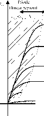 Saturation region (active region) V. increases FIGURE 6.6 (a) The -channel enhancement-mode MOSFET; and (b) its if) vs Vf)s characteristics. 6.5 MOSFET Structure Unlike the lateral channel MOSET devices used in much of the 1С technology in which the gate, source and drain terminals are located at the same surface of the silicon wafer, power MOSFETs use vertical channel structure in order to increase the device power rating [ 1 ]. In the vertical channel structure, the source and drain are on opposite side of the silicon wafer. Figure 6.7a shows a vertical cross-sectional view for a power MOSFET. Figure 6.7b shows a more simphfied representation. There are several discrete types of the vertical structure power MOSFET available commercially today, including V-MOSFET, U-MOSFET, D-MOSFET, and S-MOSFET [1, 2]. The p-n junction between the p-base (also referred to as body or bulk region) and the n-drift region provide the forward voltage blocking capabilities. The source metal contact is connected directly to the p-base region through a break in the /7+-source region in order to allow for a fixed potential to the p-base region during normal device operation. When the gate and source terminal are set to the same potential (V(3s = 0), no channel is estabhshed in the p-base region. that is, the channel region remains unmodulated. The lower doping in the /7-drift region is needed in order to achieve higher drain voltage blocking capabilities. For the drain-source current I) to flow, a conductive path must be established between the /7+- and /7~-regions through the p-base diffusion region. 6.5.1 On-State Resistance When the MOSFET is in the on-state (triode region), the channel of the device behaves like a constant resistance iDS(on) that is linearly proportional to the change between Vj) and ij) as given by the following relation: CS(on) - GS=Cons (6.1) The total conduction (on-state) power loss for a given MOSFET with forward current Ij and on-resistance iDS(on) is given by on,diss D-DS(on) (6.2) A С Metal ::y: n :: :: :sio;:; : :::: :::M   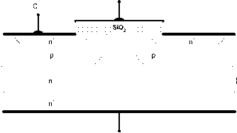 FIGURE 6.7 (a) Vertical cross-sectional view for a power MOSFET; and (b) simplified representation. The value of iDS(on) be significant and varies between tens of miUiohms and a few ohms for low-voltage and high-voltage MOSFETS, respectively. The on-state resistance is an important data sheet parameter, because it determines the forward voltage drop across the device and its total power losses. Unlike the current-controlled bipolar device, which requires base current to allow the current to flow in the collector, the power MOSFET device is a voltage-controUed unipolar device and requires only a small amount of input (gate) current. As a result, it requires less drive power than the BJT. However, it is a nonlatching current like the BJT, that is, a gate source voltage must be maintained. Moreover, as only majority carriers contribute to the current flow, MOSFETs surpass all other devices in switching speed, which switching speeds can exceed a few megahertz. Comparing the BJT and the MOSFET, the BJT has greater power handling capabilities and smaUer switching speed, while the MOSFET device has less power handling capabilities and relatively fast switching speed. The MOSFET device has a higher on-state resistor than the bipolar transistor. Another difference is that the BJT parameters are more sensitive to junction temperature when compared to the MOSFET and, unlike the BJT, MOSFET devices do not suffer from second breakdown voltages and sharing current in parallel devices is possible. 6.5.2 Internal Body Diode The modern power MOSFET has an internal diode caUed a body diode connected between the source and the drain as shown in Fig. 6.8a. This diode provides a reverse direction for the drain current, allowing a bidirectional switch implementation. Even though the MOSFET body diode has adequate current and switching speed ratings, in some power electronic applications that require the use of ultra-fast diodes, an external fast recovery diode is added in antiparallel fashion after blocking the body diode by a slow recovery diode as shown in Fig. 6.8b. 6.5.3 Internal Capacitors Another important parameter that affect the MOSFET switching behavior are the parasitic capacitances between the devices three terminals, namely, gate-to-source, Cg, gate-to-drain Cgj and drain-to-source (Q) capacitances as shown in Fig. 6.9a. The values of these capacitances are nonlinear and a function G o- Л Body diode To cancel the body diode G o- Fast recovery diode Л FIGURE 6.8 (a) MOSFET internal body diode; and (b) implementation of a fast body diode. 1 ... 5 6 7 8 9 10 11 ... 91 |
|||||||||||||||||||||||||||||||||||||||||
|
© 2026 AutoElektrix.ru
Частичное копирование материалов разрешено при условии активной ссылки |