 |
 |
 |
| Главная Журналы Популярное Audi - почему их так назвали? Как появилась марка Bmw? Откуда появился Lexus? Достижения и устремления Mercedes-Benz Первые модели Chevrolet Электромобиль Nissan Leaf |
Главная » Журналы » Metal oxide semiconductor 1 ... 81 82 83 84 85 86 87 ... 91 ;: su31 C2 su2j ;;s3j \ \ sw2 ;k swsj yv4j AC ource on inear oad FIGURE 33.6 A shunt active power fiher implemented with a three-level neutral point-clamped VSI. 33.3.2 Control Scheme The control scheme of a shunt active power filter must calculate the current reference waveform for each phase of the inverter, maintain the dc voltage constant, and generate the inverter gating signals. The block diagram of the control scheme of a shunt active power filter is shown in Fig. 33.8. The current reference circuit generates the reference currents required to compensate the load current harmonics and reactive power, and also try to maintain constant the dc voltage across the electrolytic capacitors. There are many possibilities to implement this type of control, and two of them wiU be explained in this chapter. Also, the compensation i......... ..........Jj.........l 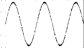 0.00 10.00 20.00 30.00 1.00 50.00  (c) (d) с rrent Control and Gating Signals Generator iac(t) ibc(t) icc(t) Gating ignals Gen Current Control Unit ia1(t) ib1(t) ic1(t) i i i a(t) b(t) c(t) iar(t) Instantaneous Act! e and React! e ower Calculation Q(t) ibr(t) icr(t) Dri er Reference Current Generator Q(t) Elimination DC component of (t) *(t) -I 4\\ oltage Control Unit DC Voltage Control С rrent Reference Generator FIGURE 33.8 The block diagram of a shunt active power filter control scheme. effectiveness of an active power filter depends on its ability to follow with a minimum error and time delay the reference signal calculated to compensate the distorted load current. Finally, the dc voltage control unit must keep the total dc bus voltage constant and equal to a given reference value. The dc voltage control is achieved by adjusting the small amount of real power absorbed by the inverter. This small amount of real power is adjusted by changing the amplitude of the fundamental component of the reference current. 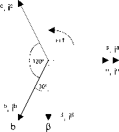 FIGURE 33.9 Transformation diagram from the a, b, с reference frame to the (X, P coordinates. where A is the transformation matrix, derived from Fig. 33.9 and is equal to 1 -1/2 -1/2 0 л/З/2 -л/З/2 (33.2) This transformation is valid if and only if v(t) + i;(t) + vt) is equal to zero, and also if the voltages are balanced and sinusoidal. The instantaneous active and reactive power in the ot-j] coordinates are calculated with the following expressions: 33.3.2.1 Current Reference Generation There are many possibilities to determine the reference current required to compensate the nonlinear load. Normally, shunt active power filters are used to compensate the displacement power factor and low frequency current harmonics generated by nonhnear loads. One alternative to determine the current reference required by the voltage-source inverter is the use of the instantaneous reactive power theory, proposed by Akagi [1]. This concept is very popular and useful for this type of apphcation, and basically consists of a variable transformation from the a,b, с reference frame of the instantaneous power, voltage and current signals to the a, reference frame. The transformation equations from the a,b, с reference frame to the a, coordinates can be derived from the phasor diagram shown in Fig. 33.9. The instantaneous values of voltages and currents in the a, j] coordinates can be obtained from the following equations: = [A]. = [A]. (33.1) P(0 = ta(04(0 + tOO (33.3) (lit) = -v,(t)ip(t) + vp(t\(t) (33.4) It is evident that p(t) becomes equal to the conventional instantaneous real power defined in the a, b, с reference frame. However, in order to define the instantaneous reactive power, Akagi introduces a new instantaneous space vector defined by expression (33.4) or by the vector equation: (33.5) The vector q is perpendicular to the plane of a, coordinates, to be faced in compliance with a right-hand rule, and v is perpendicular to i, and г; is perpendicular to i. The physical meaning of the vector q is not instantaneous power because of the product of the voltage in one phase and the current in the other phase. On the contrary, vj and in Eq. (33.3) obviously mean instantaneous power because of the product of the voltage in one phase and the current in the same phase. Akagi named the new electrical quantity defined in (33.5) instantaneous imaginary power , which is represented by the product of the instantaneous voltage and current, but cannot be treated as a conventional quantity. The expression of the currents in the a- plane, as a function of the instantaneous power is given by the foUowing equation: Vr -V, (33.6) and the different components of the currents in the a, plane are shown in the foUowing expressions: iRf. = vlvj vl + vj vlvj vlvl (33.7) (33.8) (33.9) (33.10) From Eqs. (33.3) and (33.4), the values of p and q can be expressed in terms of the dc components plus the ac components, that is: p=~p + p q=~q + q (33.11) (33.12) where p: dc component of the instantaneous power p, and is related to the conventional fundamental active current. p: is the ac component of the instantaneous power p, it does not have average value, and is related to the harmonic currents caused by the ac component of the instantaneous real power. q;. is the dc component of the imaginary instantaneous power q, and is related to the reactive power generated by the fundamental components of voltages and currents. q: is the ac component of the instantaneous imaginary power q, and is related to the harmonic currents caused by the ac component of instantaneous reactive power. In order to compensate reactive power (displacement power factor) and current harmonics generated by nonlinear loads, the reference signal of the shunt active power filter must include the values of p, , and q. In this case the reference currents required by the shunt active power filters are calculated with the foUowing expression: (33.13)
The final compensating currents including the zero sequence components in a,b, с reference frame are the foUowing: 1 -1 л/З 7! 1 -1 -л/З 2 j (33.14) where the zero sequence current component Zq is equal to 1/а/З (*д + ц + ic) The block diagram of the circuit required to generate the reference currents defined in (33.14) is shown in Fig. 33.10. The advantage of p-q theory is that real and reactive power associated with fundamental components are dc quantities. These quantities can be extracted with a low pass filter. Since the signal to be extracted is dc, filtering of the signal in the Transformation Transformation wit Zero equence p and q calculation In erse ark Transform К с rrent Control Unit Generated Current oad Current -
Reference Current Current Controller oad Current econd Order Filter (50 or 60 Hz) eak alue Gating ignals Generator Dc generated
С rrent Reference Generator Dc Control Unit FIGURE 33.11 The block diagram of an active power filter control scheme that does not use the instantaneous reactive power concept. a-P reference frame is insensitive to any phase shift errors introduced by the low pass filter, improving compensation characteristics of the active power filter. The same advantage can be obtained by using the Synchronous Reference Frame Method, proposed in [2]. In this case transformation from a, h, с axes to d-q synchronous reference frame is done. There are other possibilities to generate the current reference signal required to compensate reactive power and current harmonics. Basically, all the different schemes try to obtain the current reference signals that include the reactive components required to compensate the displacement power factor and the current harmonics generated by the nonlinear load. Figure 33.11 shows another scheme used to generate the current reference signals required by a shunt active power filter. In this case the ac current generated by the inverter is forced to follow the reference signal obtained from the current reference generator. In this circuit, the distorted load current is filtered, extracting the fundamental component, i. The band-pass filter is tuned at the fundamental frequency (50 or 60 Hz), so that the gain attenuation introduced in the filter output signal is zero and the phase-shift angle is 180°. Thus, the filter output current is exactly equal to the fundamental component of the load current but phase shifted by 180°. If the load current is added to the fundamental current component obtained from the second order band-pass filter, the reference current waveform required to compensate only harmonic distortion is obtained. In order to provide the reactive power required by the load, the current signal obtained from the second order band-pass filter J/i, is synchronized with the respective phase-to-neutral source voltage (see Fig. 33.12) so that the inverter ac output current is forced to lead the respective inverter output voltage, thereby generating the required reactive power and absorbing the real power necessary to supply the switching losses and also to maintain the dc voltage constant (see Fig. 33.12). The real power absorbed by the inverter is controlled by adjusting the amplitude of the fundamental current reference waveform, I, obtained from the reference current generator. The amplitude of this sinusoidal waveform is equal to the amplitude of the fundamental component of the load current plus or minus the error signal obtained from the dc voltage control unit. In this way, the current signal allows the inverter to supply the current harmonic components, the reactive power required by the load, and to absorb the small amount of active power necessary to cover the switching losses and to keep the dc voltage constant. 33.3.2.2 Current Modulator The effectiveness of an active power filter depends basically on the design characteristics of the current controller, the method implemented to generate the reference template and the modulation technique used. Most of the modulation techniques used in active power filters are based on PWM strategies. In this chapter, four of these methods, whose characteristics are their simplicity and effectiveness, are analyzed: Periodical Sampling Control, Hysteresis Band Control, Triangular Carrier Control, and Vector Control. The first three methods have been tested with different waveform templates sinusoidal, quasisquare and rectifier compensation current and were compared in terms of the harmonic content and distortion at the same switching frequency [3]. The analysis shows that (a) (b) FIGURE 33.12 The procedure for the generation of the current reference waveform, (a) The load current /а its fundamental component, {ц, and the fundamental current component synchronized with the respective phase-to-neutral source voltage, ц^. (b) The synchronized fundamental current signal minus the load current, - /iad and its fundamental component. for sinusoidal current generation the best method is Triangular Carrier, foUowed by the Hysteresis Band and Periodical Sampling. For other types of references, however, one strategy may be better than the others. Also it was shown that each control method is affected in a different way by the switching time delays present in the driving circuitry and in the power semiconductors. The Periodical Sampling method switches the power transistors of the converter during the transitions of a square wave clock of fixed frequency (the sampling frequency) As shown in Fig. 33.13(a), this type of control is very simple to implement since it requires a comparator and a D-type flip-flop per phase. The main advantage of this method is that the minimum time between switching transitions is limited to the period of the samphng clock. Fiowever, the actual switching frequency is not clearly defined. The Fiysteresis Band method switches the transistors when the current error exceeds a fixed magnitude: the hysteresis band. As can be seen in Fig. 33.13(b), this type of control needs a single comparator with hysteresis per phase. In this case the switching frequency is not determined, but it can be estimated. The Triangular Carrier method, shown in Fig. 33.13(c), compares the current error with a fixed amplitude and fixed frequency triangular wave (the triangular carrier). The error is processed through a proportional-integral (PI) gain stage before the comparison with the triangular carrier takes place. As can be seen, this control scheme is more complex than the Periodical Sampling and Fiysteresis Band. The values for the PI control gain kp and k determine the transient response and steady-state error of the Triangular Carrier method. It was found empirically that the values for kp and k shown in Eqns.
/I hysteresis band adjust  IJine I err 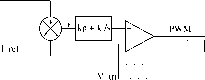 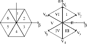 (a) (b) FIGURE 33.14 The hexagons defined in the a- reference frame by the current control scheme, (a) The hexagon defined by the inverter output current vector, (b) The hexagon defined by the inverter output voltage vector. (33.15) and (33.16) give a good dynamic performance under transient and steady-state operating conditions: fc = (1 + 1о)-ш, 2к (33.15) (33.16) where T + Tq is the total series inductance seen by the converter, o) is the triangular carrier frequency, which amphtude is one volt peak-peak, and V is the dc supply voltage of the inverter. 33,3,2,2,1 Vector Control Technique This current control technique proposed in [4] divides the a-P reference frame of currents and voltages in six regions, phase-shifted by 30° (Fig. 33.14), identifies the region where the current vector error Ai is located, and selects the inverter output voltage vector V that wiU force Ai to change in the opposite direction, keeping the inverter output current close to the reference signal. Figure 33.15 shows the single phase equivalent circuit of the shunt active power filter connected to a nonhnear load and to the power supply. ower upply 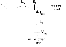 The equation that relates the active power filter currents and voltages is obtained by applying Kirchhoff law to the equivalent circuit shown in Fig. 33.15: -gen (33.17) The current error vector Ai is defined by the following expression: (33.18) where represents the inverter reference current vector defined by the instantaneous reactive power concept. By replacing (33.18) in (33.17): + £o-in If £ = L(di,f/dt) + then (2.20) becomes (33.19) (33.20) Equation (33.20) represents the active power fiher state equation and shows that the current error vector variation dAi/dt is defined by the difference between the fictitious voltage vector E and the inverter output voltage vector V. In order to keep dAi/dt close to zero, У^у niust be selected near E. The selection of the inverters gating signals is defined by the region in which Ai is located and by its amplitude. In order to improve the current control accuracy and associate time response, depending on the amplitude of Ai the following actions are defined: - if Ai < the gating signals of the inverter are not changed, - if h < Ai < 3, the inverter gating signals are defined following Mode a, - if Ai > h, the inverter gating signals are defined following Mode b 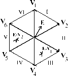 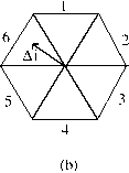 FIGURE 33.16 Selection of the inverter switching pattern according to the region where Ai and E are located, (a) The regions where LdAi/dt are located, (b) The region where Ai is located. where 3 and h are reference values that defines the accuracy and the hysterisis window of the current control scheme. Mode a: Small Changes in Ai(h < Ai < 3) The selection of the inverter switching Mode a can be explained with the following example. Assuming that the voltage vector E is located in region I (Fig. 33.16(a)) and the current error vector Ai is in region 6 (Fig. 33.16(b)) the inverter voltage vectors, ynv located closest to E are and V2. The vectors E - V2 and E - Vl define two vectors LdAi/dt, located in region III and V respectively, as shown in Fig. 33.15(a), so in order to reduce the current vector error Ai, LdAi/dt must be located in region III. Thus the inverter output voltage has to be equal to У^. In this way Ai will be forced to change in the opposite direction, reducing its amplitude faster. By doing the same analysis for all the possible combinations, the inverter switching modes for each location of Ai and E can be defined (Table 33.2). Vj represents the inverter switching functions defined in Table 33.3. Mode b: Large Changes in Ai(Ai > h) If Ai becomes larger than /г in a transient state, it is necessary to choose the switching mode in which the dAi/dt has the largest opposite direction to Ai. In this case the best inverter output voltage ynv corresponds to the value located in the same region of Ai. The switching frequency may be fixed by controlling the time between commutations and by not applying a new TABLE 33.2 Inverter switching modes E Region Ai Region 1
TABLE 33.3 Relationship between switching function and inverter output voltage Switch on Phase a Switch on Phase b Switch on Phase с Inverter Output Voltage Vj switching pattern if the time between two successive commutations is lower than a selected value (t = f). Figure 33.17 shows the block diagram of the inverter vector current control scheme implemented in a microcontroUer. In Fig. 33.17 E represents the region where the vector E is located, Ai the region of Ai, ki keeps the same value of /с (no commutation in the inverter), selects the new inverter output voltage from Table 33.2, and k selects У^у the same region of Ai. 33.3.2.3 Control loops Design Active power filters based on self controUed dc bus voltage requires two control loops, one to control the inverter output current and the other to regulate the inverter dc voltage. Different design criteria have been presented in the technical literature; however, a classic design procedure using a PI controller wiU be presented in this chapter. In general, the design procedure for the current and voltage loops is based on the respective time response requirements. Since the transient response of the active power is determined by the current control loop, its time response has to be fast enough to foUow the current reference waveform closely. On the other hand, the time response of the dc voltage does not need to be fast and is selected to be at least ten times slower than the current control Previous k2 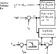 5 < Ai < h Vinv selected from Table I
I k1 Defines Switching Mode Selects kl, k2 or кЗ loop time response. Thus, these two control systems can be decoupled and designed as two independent systems. A PI controUer is normally used for the current and the voltage control loops since it contributes to zero steady-state error in tracking the reference current and voltage signals, respectively. 33,3,2,3,1 Design of the Current Control Loop The design of the current control loop gains depends on the selected current modulator. In the case of selecting the triangular carrier technique, to generate the gating signals, the error between the generated current and the reference current is processed through a PI controUer, then the output current error is compared with a fixed amplitude and fixed frequency triangular wave (Fig. 33.13(c)) The advantage of this current modulator technique is that the output current of the converter has weU defined spectral line frequencies for the switching frequency components. Since the active power filter is implemented with a voltage-source inverter, the ac output current is defined by the inverter ac output voltage. The block diagram of the current control loop for each phase is shown in Fig. 33.18 where E phase to neutral source voltage, Z(s) impedance of the link reactor, gain of the converter, Gc(s) gain of the controUer. The values of and Gc(s) are given in (33.21) and (33.22). Gc(s) = Kp s (33.21) (33.22) From Fig. 33.18 and (33.22), the following expression is obtained: E (33.23) Gc(s) Z(s) The characteristic equation of the current loop is given by (33.24) The analysis of the characteristic equation proves that the current control loop is stable for all values of Kp and K. Also, this analysis shows that Kp determines the speed response and Ki defines the damping factor of the control loop. If Kp is too big, the error signal can exceed the amplitude of the triangular waveform, affecting the inverter switching frequency, and if K is too small, the gain of the PI controller decreases, which means that the generated current will not be able to follow the reference current closely. The active filter transient response can be improved by adjusting the gain of the proportional part {Kp) to equal one and the gain of the integrator {K) to equal the frequency of the triangular waveform. 33.3.2.3.2 DC Voltage Control Loop Vohage control of the dc bus is performed by adjusting the small amount of real power flowing into the dc capacitor, thus compensating for the conduction and switching losses. The voltage loop is designed to be at least 10 times slower than the current loop; hence the two loops can be considered decoupled. The dc voltage control loop needs not to be fast, since it only responds for steady-state operating conditions. Transient changes in the dc voltage are not permitted and are taken into consideration with the selection criteria of the appropriate electrolytic capacitor value. modulator is used. The design of the synchronous reactor is performed with the constraint that, for a given switching frequency, the minimum slope of the inductor current is smaller than the slope of the triangular waveform that defines the switching frequency. In this way, the intersection between the current error signal and the triangular waveform will always exist. In the case of using another current modulator, the design criteria must allow an adequate value of L in order to ensure that the di/dt generated by the active power filter will be able to follow the inverter current reference closely. In the case of the triangular carrier technique, the slope of the triangular waveform, Я, is defined by (33.25) where is the amplitude of the triangular waveform, which has to be equal to the maximum permitted amount of ripple current, and fi is the frequency of the triangular waveform (i.e., the inverter switching frequency). The maximum slope of the inductor current is equal to (33.26) Since the slope of the inductor current (dii/dt) has to be smaller than the slope of the triangular waveform (Я), and the ripple current is defined, from (33.25) and (33.26), as 33.3.3 Power Circuit Design The selection of the ac link reactor and the dc capacitor values affects directly the performance of the active power filter. Static var compensators implemented with voltage-source inverters present the same power circuit topology, but for this type of apphcation, the criteria used to select the values of Lj. and С are different. For reactive power compensation, the design of the synchronous link inductor, L., and the dc capacitor, C, is performed based on harmonic distortion constrain. That is, L must reduce the amplitude of the current harmonics generated by the inverter while С must keep the dc voltage ripple factor below a given value. This design criteria cannot be applied in the active power filter since it must be able to generate distorted current waveforms. However, L must be specified so that it keeps the high-frequency switching ripple of the inverter ac output current smaller than a defined value. 33.3.3.1 Design of the Synchronous Link Reactor The design of the synchronous link reactor depends on the current modulator used. The design criteria presented in this section is based on considering that the triangular carrier (33.27) 33.3.3.2 Design of the DC Capacitor Transient changes in the instantaneous power absorbed by the load generate voltage fluctuations across the dc capacitor. The amplitude of these voltage fluctuations can be controlled effectively with an appropriate dc capacitor value. It must be noticed that the dc voltage control loop stabilizes the capacitor voltage after a few cycles, but is not fast enough to limit the first voltage variations. The capacitor value obtained with this criteria is bigger than the value obtained based on the maximum dc voltage ripple constraint. For this reason, the voltage across the dc capacitor presents a smaller harmonic distortion factor. The maximum overvoltage generated across the dc capacitor is given by Vr =- ic(t)dt+V (33.28) where V is the maximum voltage across the dc capacitor, Vj3 is the steady-state dc voltage, and iit) is the instantaneous dc bus current. From (33.28) 62/(0 ic(t)dt (33.29) Eqn. (33.29) defines the value of the dc capacitor, C, that wiU maintain the dc voltage fluctuation below A У p.u. The instantaneous value of the dc current is defined by the product of the inverter line currents with the respective switching functions. The mean value of the dc current that generates the maximum overvoltage can be estimated by 62/CD ic(t)dt = в2/С0 [sin{(Dt) + sm{(Dt + 120°)]/: (33.30) In this expression the inverter ac current is assumed to be sinusoidal. These operating conditions represent the worst case. 33.3.4 Technical Specifications The standard specifications of shunt active power filters are the foUowing: Number of phases: 3-phase and three wires or 3-phases and four wires. Input voltage: 200, 210, 220 ±10%, 400, 420, 440 ib%, 6600 ±10%. Frequency: 50/60 Hz ±5%. No. of restraint harmonic orders: 2-25 th. Harmonic restraint factor: 85% or more at the rated output. Type of rating: continuous. Response: 1 ms or less. For shunt active power filter the harmonic restraint factor is defined as (1 = I/I) x 100%, where 1щ are the harmonic currents flowing on the source side when no measure are taken for harmonic suppression, and 1щ are the harmonic currents flowing on the source side when harmonics are suppressed using an active filter. 33.4 Series Acrive Power Filters Series active power filters were introduced by the end of the 1980s [5], and operate mainly as a voltage regulator and as harmonic isolator between the nonlinear load and the utility system. The series connected active power filter is more preferable to protect the consumer from an inadequate supply voltage quality. This type of approach is specially eries Acti e Filter sys. AC - upply Compensation oltage FIGURE 33.19 The series active power fiher operating as a vohage compensator. recommended for compensation of voltage unbalances and voltage sags from the ac supply, and for low power applications represents an economically attractive alternative to UPS, since no energy storage (battery) is necessary and the overaU rating of the components is smaUer. The series active power filter injects a voltage component in series with the supply voltage and therefore can be regarded as a controUed voltage source, compensating voltage sags and sweUs on the load side (Fig. 33.19). If passive LC filters are connected in paraUel to the load, the series active power filter operates as an harmonic isolator forcing the load current harmonics to circulate mainly through the passive filter rather than the power distribution system (hybrid topology). The main advantage of this scheme is that the rated power of the series active power filter is a smaU fraction of the load kVA rating, typically 5%. However, the rating apparent power of the series active power filter may increase in case of voltage compensation. 33.4.1 Power Circuit Structure The topology of the series active power filter is shown in Fig. 33.20. In most cases, the power circuit configuration is based eries Acti e Filter 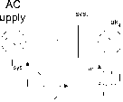 on linear oad
assi e Filter  - Й Й Й assi e Filter Three-hase -V j ie Filter ( cti e о er ilter) FIGURE 33.21 The series active power filter topology. on a three-phase PWM voltage-source inverter connected in series with the power lines through three single-phase coupling transformers. For certain type of applications, the three-phase PWM voltage-source converter can be replaced by three single phase PWM inverters. However, this type of approach requires more power components, which increases the cost. In order to operate as an harmonic isolator, a parallel LC filter must be connected between the nonlinear loads and the coupling transformers (Fig. 33.21) Current harmonic and voltage compensation are achieved by generating the appropriate voltage waveforms with the three-phase PWM voltage-source inverter, which are reflected in the power system through three coupling transformers. With an adequate control scheme series active power filters can compensate for current harmonics generated by nonlinear loads, voltage unbalances and voltage sags or swells at the load terminals. However, it is very difficult to compensate the load power factor with this type of topology. In four-wire power distribution systems, series active power filters with the power topology shown in Fig. 33.21 can also compensate the current harmonic components that circulate through the neutral conductor. 33.4.2 Principles of Operation Series active power filters compensate current system distortion caused by nonlinear loads by imposing a high impedance path to the current harmonics, which forces the high frequency currents to flow through the LC passive filter connected in parallel to the load (Fig. 33.20) The high impedance imposed by the series active power filter is created by generating a voltage of the same frequency that the current harmonic component that needs to be eliminated. Voltage regulation or voltage unbalance can be corrected by compensating the fundamental frequency positive, negative and zero sequence voltage components of the power distribution system (Fig. 33.19). In this case, the series active power filter injects a voltage component in series with the supply voltage and therefore can be regarded as a controlled voltage source, compensating voltage regulation on the load side (sags or swells), and voltage unbalance. Voltage injection of arbitrary phase with respect to the load current implies active power transfer capabilities which increases the rating of the series active power filter. Voltage and current waveforms shown in Figs. 33.22, 33.23, and 33.24 illustrate the compensation characteristics of a series active power filter operating with a shunt passive filter. 33.4.3 Power Circuit Design The power circuit topology of the series active power filter is composed by the three-phase PWM voltage source inverter, the second order resonant LC filters, the couphng transformers, and the secondary ripple frequency filter (Fig. 33.21) The design characteristics for each of the power components are described below. 33.4.3.1 PWM Voltage-Source Inverter Since series active power filter can compensate voltage unbalance and current harmonics simultaneously, the rated power of the PWM voltage-source inverter increases compared with other approaches that compensate only current harmonics, since voltage injection of arbitrary phase with respect to the load current imphes active power transfer from the inverter to the system. Also, the transformer leakage inductance entails -2 V 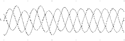 FIGURE 33.22 Load voltage waveforms for voltage unbalance compensation. Phase to neutral voltages at the load terminals before and after series compensation. (Compensation starts at 140 ms, current harmonic compensator not operating). 1 ... 81 82 83 84 85 86 87 ... 91 |
||||||||||||||||||||||||||||||||||||||||||||||||||||||||||||||||||||||||||||||||||||||||||||||||||||||||||||||||||||||||||||||||||||||||||||||||||||||||||||||
|
© 2026 AutoElektrix.ru
Частичное копирование материалов разрешено при условии активной ссылки |