 |
 |
 |
| Главная Журналы Популярное Audi - почему их так назвали? Как появилась марка Bmw? Откуда появился Lexus? Достижения и устремления Mercedes-Benz Первые модели Chevrolet Электромобиль Nissan Leaf |
Главная » Журналы » Metal oxide semiconductor 1 ... 82 83 84 85 86 87 88 ... 91 - .A 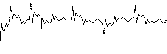 -2 A
Time FIGURE 33.23 System current waveforms for current harmonic compensation, (a) Neutral current flowing to the ac mains before and after compensation, (b) Line currents flowing to the ac mains before and after compensation. (Voltage unbalance compensator not operating). fundamental voltage drop and fundamental apparent power, which has to be supported by the inverter, reducing the series active filter inverter rating available for harmonic and voltage compensation. The rated apparent power required by the inverter can be obtained by calculating the apparent power generated in the primary of the coupling transformers. The voltage reflected across the primary winding of each coupling transformer is defined by the following expression: V = series у/2 11/2 (33.31) 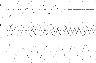 FIGURE 33.24 Load voltages and system currents for voltage unbalance and current harmonic compensation, before and after compensation, (a) Power system neutral current, (b) Phase-to-neutral load voltages, (c) Power system line current. where Vi is the rms voltage across the primary winding of the coupling transformer. Equation (33.31) shows that the voltage across the primary winding of the transformer is defined by two terms. The first one is inversely proportional to the quality factor of the passive LC filter, while the second one depends on the voltage unbalance that needs to be compensated. depends on the LC filter values while K2 is equal to one. The current flowing through the primary winding of the couphng transformer, due to the harmonic currents (Eqn. (33.32)), can be obtained from the equivalent circuit shown in Fig. 33.25: fkhk (33.32) where Vi = -К^!. The fundamental component of the primary current depends on the amplitude of the negative and zero sequence component of the source voltage due to the system unbalance. oadk FIGURE 33.25 The equivalent circuit of the series active power filter for harmonic components. 33.4.3.2 Coupling Transformer The purpose of the three couphng transformers is not only isolate the PWM inverters from the source but also to match the voltage and current ratings of the PWM inverters with those of the power distribution system. The total apparent power required by each coupling transformer is 1/3 the total apparent power of the inverter. The turn ratio of the current transformer is specified according to the inverter dc bus voltage, Ki and V. The correct value of the turn ratio a must be specified according to the overall series active power filter performance. The turn ratio of the coupling transformer must be optimized through the simulation of the overall active power filter, since it depends on the values of different related parameters. In general, the transformer turn ratio must be high in order to reduce the amplitude of the inverter output current and to reduce the voltage induced across the primary winding. Also, the selection of the transformer turn ratio influences the performance of the ripple filter connected at the output of the PWM inverter. Taking into consideration all these factors, in general, the transformer turn ratio is selected equal to 1:20. ter output voltage must be almost equal to the voltage across Cfj.. However, for high frequency components, most of the inverter output voltage must drop across Lf., in which case the voltage at the capacitor terminals is almost zero. Moreover, Cf. and Lfj. must be selected in order not to exceed the burden of the coupling transformer. The ripple filter must be designed for the carrier frequency of the PWM voltage-source inverter. To calculate Cfj. and the system equivalent impedance at the carrier frequency, Zg, reflected in the secondary must be known. This impedance is equal to sys(secondary) sys(primary) (33.33) For the carrier frequency, the following design criteria must be satisfied: (i) Xfr Lfr to ensure that at the carrier frequency most of the inverter output voltage will drop across Ц^. (ii) Xcfr and to ensure that the voltage divider is Lfr < sys between and Cf.. 33.4.3.3 Secondary Ripple Filter The design of the ripple filter connected in parallel to the secondary winding of the couphng transformer is performed following the method presented by Akagi in [6]. However, it is important to notice that the design of the secondary ripple filter depends mainly on the coupling transformer turn ratio and on the current modulator used to generate the inverter gating signals. If the triangular carrier is used, the frequency of the triangular waveform has to be considered in the design of the ripple filter. The ripple filter connected at the output of the inverter avoid the induction of the high frequency ripple voltage generated by the PWM inverter switching pattern at the terminals of the primary winding of the coupling transformer. In this way, the voltage apphed in series to the power system corresponds to the components required to compensate voltage unbalanced and current harmonics. The single-phase equivalent circuit is shown in Fig. 33.26. The voltage reflected in the primary winding of the current transformer has the same waveform that the voltage across the filter capacitor has. For low frequency components, the inver- -sys The small-rated LC passive filter exhibits a high quality factor circuit because of the high impedance on the output side. Oscillation between the small rated inductor and capacitor may occur, causing undesirable high frequency voltage across the ripple filter capacitor, which is reflected in the primary winding of the coupling transformer generating high frequency current to flow through the power distribution system. It is important to note that this oscillation is very difficult to eliminate through the design and selection of the Lfj. and Cfj. values. However, it can be eliminated with the addition of a new control loop. The cause of the output voltage oscillation is explained with the help of Fig. 33.27. The transfer function Gp{s) between the input voltage У^(5) and the output voltage Vc{s) is given by the equation: s2 + 2io + ml (33.34) where co = .JVJI and = {rJ2)/(CjL. 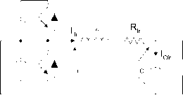 Cfr® Is FIGURE 33.26 The single-phase equivalent circuit of the inverter FIGURE 33.27 Single-phase equivalent circuit of series active power output ripple filter. filter connected to the ripple filter. Normally, the damping factor is smaUer than one, causing the voltage osciUation across the capacitor ripple filter, Q. Generally, relatively low impedance loads are connected to the output terminals of voltage source PWM inverters. In these cases, the quality factor of the LC filter can be low, and the osciUation between the inductor L and the capacitor Cfj. is avoided [7]. 33.4.3.4 Passive Filters Passive filters connected between the nonlinear load and the series active power play an important role in the compensation of the load current harmonics. With the connection of the passive filters the series active power filter operates as an harmonic isolator. The harmonic isolation feature reduces the need for precise tuning of the passive filters and aUows their design to be insensitive to the system impedance and ehminates the possibility of filter overloading due to supply voltage harmonics. The passive filter can be tuned to the dominant load current harmonic and can be designed to correct the load displacement power factor. However, for industrial loads connected to stiff supply, it is difficult to design passive filters that can absorb a significant part of the load harmonic current and therefore its effectiveness deteriorates. Specially, for compensation of diode rectifier type of loads, where a smaU kvar passive filter is required, it is difficult to achieve the required tuning to absorb significant percentage of the load harmonic currents. For this type of apphcation, the passive filters cannot be tuned exactly to the harmonic frequencies because they can be overloaded due to the system voltage distortion and/or system current harmonics. The single-phase equivalent circuit of a passive LC filter connected in paraUel to a nonlinear current source and to the power distribution system is shown in Fig. 33.28. From this figure, the design procedure of this filter can be derived. The harmonic current component flowing through the passive filter ij and the current component flowing through the source i/j are given by the foUowing expressions: fh = t.h = - Zs + Zf (33.35) 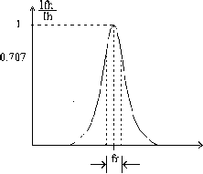 f[Hz] FIGURE 33.29 The passive fiher bandwidth. At the resonant frequency the inductive reactance of the passive filter is equal to the capacitive reactance of the filter, that is: InfrL = InfrC (33.36) Therefore, the resonant frequency of the passive filter is equal to: fr = 2ял/1С' (33.37) The passive filter band width is defined by the upper and lower cutoff frequency, at which values the filter current gain is -3 dB, as shown in Fig. 33.29. The magnitude of the passive filter impedance as a function of the frequency is shown in Fig. 33.30. At the resonant frequency the passive filter magnitude is equal to the resistance. If the resistance is zero, the filter is in short circuit. The quality factor of the passive filter is defined by the foUowing expression: (33.38) 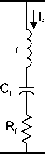 It is important to note that the operation of the series active power fiher with off-tuned passive fiher has an adverse impact on the inverter power rating compared to the normal case. The more off-tuned the passive filter is the more rated apparent power is required by the series active power filter. 33.4.3.5 Protection Requirements Short circuits in the power distribution system generate large currents that flow through the power fines until the circuit breaker operates clearing the fault. The total clearing time of a short circuit depends on the time delay imposed by the protection system. The clearing time cannot be instantaneous due to the operating time imposed by the overcurrent relay and by the total interruption time of the power circuit breaker. Although power system equipment, such us power transformers, cables, etc., are designed to withstand short-circuit currents during at least 30 cycles, the active power filter may suffer severe damage during this short time. The withstand capability of the series active power filter depends mainly on the inverter power semiconductor characteristics. Since the most important feature of series active power filters is the small rated power required to compensate the power system, typically 10-15% of the load rated apparent power, the inverter semiconductors are rated for low values of blocking voltages and continuous currents. This makes series active power filters more vulnerable to power system faults. The block diagram of the protection scheme described in this section is shown in Fig. 33.31. It consists of a varistor connected in parallel to the secondary winding of each coupling transformer, and a couple of antiparallel thyristors [8]. A special circuit detects the current flowing through the varistors and generates the gating signals of the antiparallel thyristors. The protection circuit of the series active power filter must protect only the PWM voltage-source inverter connected to the secondary of the coupling transformers and must not interfere with the protection scheme of the power distribution system. Since the primary of the active power filter couphng transformers are connected in series to the power distribution system, they operate as current transfor- 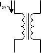 / О 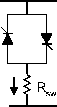 Control Circuit ws FIGURE 33.31 The series active power fiher protection scheme. mers, so that their secondary windings cannot operate in open circuit. For this reason, if a short-circuit is detected in the power distribution system, the PWM voltage-source inverter cannot be disconnected from the secondary of the current transformer. Therefore, the protection scheme must be able to limit the amplitude of the currents and voltages generated in the secondary circuits. This task is performed by the varistors and by the magnetic saturation characteristic of the transformers. The main advantages of the series active power filter protection scheme described in this section are the following: i) it is easy to implement and has a reduced cost, ii) it offers full protection against power distribution short-circuit currents, iii) it does not interfere with the power distribution system. When short-circuit currents circulate through the power distribution system, the low saturation characteristic of the transformers increases the current ratio error and reduces the amplitude of the secondary currents. The larger secondary voltages induced by the primary short-circuit currents are clamped by the varistors, reducing the amplitude of the PWM voltage-source inverter currents. After a few cycles of duration of the short-circuit, the PWM voltage-source inverter is bypassed through a couple of antiparallel thyristors, and at the same time the gating signals applied to the PWM voltage-source inverter are removed. In this way, the PWM voltage-source inverter can be turned off. The principles of operation and the effectiveness of the protection scheme are shown in Fig. 33.32. The secondary short-circuit currents will circulate through the antiparallel thyristors and the varistors until the fault is cleared by the protection equipment of the power distribution system. By using the protection scheme described in this subsection, the voltage and currents reflected in the secondary of the couphng transformers are significantly reduced. When short-circuit currents circulate through the power distribution system, the low saturation characteristic of the coupling transformers increases the current ratio error and reduces the amplitude of the secondary voltages and currents. Moreover, the saturated high secondary voltages induced by the primary short-circuit currents are clamped by the varistors, reducing the amplitude of the PWM voltage-source inverter ac currents. Once the secondary current exceeds a predefined reference value, the PWM voltage-source inverter is by-passed through a couple of antiparallel thyristors, and then the gating signals applied to the PWM voltage-source inverter are removed. The effectiveness of the protection scheme is shown in Fig. 33.33. By increasing the current ratio error due to the magnetic saturation, the energy dissipated in the secondary of the couphng transformer is significantly reduced. The total 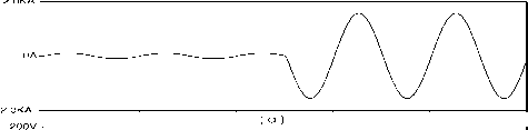 80ms 100ms Time 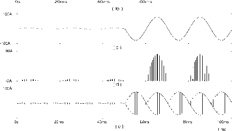 -100 A FIGURE 33.32 Current waveforms of the series active power fiher during a three-phase short-circuit in the power distribution system set at 50 ms. (a) Power distribution system line current, (b) Current transformer secondary voltage, (c) Inverter ac current, (d) Current through an inverter leg. (e) Inverter dc bus current. -10A 20 A -20A 10A
100ms Time FIGURE 33.33 Current waveforms for a line to line short-circuit in the power distribution system. The protection scheme is implemented with the varistor, a couple of antiparallel thyristors, and a coupling transformer with low saturation characteristic, (a) Current through the varistor. (b) Current through the thyristors. (c) Inverter ac current. energy dissipated in the varistor for the different protection conditions is shown in Fig. 33.34. 33.4.4 Control Issues The block diagram of a series active power filter control scheme that compensates current harmonics and voltage unbalance simultaneously is shown in Fig. 33.35. Current and voltage reference waveforms are obtained by using the Park Transformation (Instantaneous Reactive Power Theory). Voltage unbalance is compensated by calculating the negative and zero sequence fundamental components of the system voltages. These voltage components are added to the source voltages through the coupling transformers compensating the voltage unbalance at the load terminals. In order to reduce the amplitude of the current flowing through the neutral conductor, the zero sequence components of the line Energy [Joule] 100-80- The vohages v, Vy, and correspond to the power system phase to neutral voltages before the current transformer. The reference voltage signals are obtained by making the positive sequence component, v zero and then applying the inverse of the Fortescue transformation. In this way the series active power filter compensates only voltage unbalance and not voltage regulation. The reference signals for the voltage unbalance control scheme are obtained by applying the following equations: Type of Protection FIGURE 33.34 The total energy dissipated in the varistor during the power system short-circuit for different protection schemes implementations, (a) Only with the varistor used, (b) The varistor is connected in paraUel to a bidirectional switch, (c) With the complete protection scheme operating (including the coupling transformer with low saturation characteristics). Voltage eference eneratorfor rrent ar onics о pensation rans ormation V V, v Calculation о pand q P(t) Pref igh ass ilter In erse ar rans ormation к Fundamental olta e e uence Com onents
atin i nals enerator Voltage eference enerator for n alance о pensation FIGURE 33.35 Compensation scheme for voltage unbalance correction. currents are calculated. In this way, it is not necessary to sense the current flowing through the neutral conductor. 33.4.4.1 Reference Signals Generator The compensation characteristics of series active power filters are defined mainly by the algorithm used to generate the reference signals required by the control system. These reference signals must allow current and voltage compensation with minimum time delay. Also it is important that the accuracy of the information contained in the reference signals allows the elimination of the current harmonics and voltage unbalance presents in the power system. Since the voltage and current control scheme are independent, the equations used to calculate the voltage reference signals are the following: 7з 1 1 1 1 a a 1 a a (33.39) refa refb refc (33.40) In order to compensate current harmonics generated by the nonlinear loads, the following equations are used: -1/2 V3/2 -1/2 -v3/2
(33.41) where iq is the fundamental zero sequence component of the hne current and is calculated using the Fortescue transformation: io = (l/V3)(4 + ib + ic). (33.42) In (33.41) v, and are defined according to the Instantaneous Reactive Power Theory. In order to avoid the compensation of the zero sequence fundamental frequency current the reference signal iq must be forced to circulate through a high pass filter generating a current iq which is used to create the reference signal required to compensate current harmonics. Finally, the general equation that defines the references of the PWM voltage-source inverter required to compensate voltage unbalance and current harmonics is the following:
J L-a2j (33.43) where is the gain of the couphng transformer which defines the magnitude of the impedance for high frequency current components, and K2 defines the degree of compensation for vohage unbalance, (ideally К2 equals 1). 33.4.4.2 Gating Signals Generator This circuit provides the gating signals of the three-phase PWM voltage-source inverter required to compensate voltage unbalance and current harmonic components. The current and voltage reference signals are added and then the amplitude of the resultant reference waveform is adjusted in order to increase the voltage utilization factor of the PWM inverter for steady-state operating conditions. The gating signals of the inverter are generated by comparing the resultant reference signal with a fixed frequency triangular waveform. The triangular waveform helps to keep the inverter switching frequency constant (Fig. 33.36). A higher voltage utilization of the inverter is obtained if the amplitude of the resultant reference signal is adjusted for the steady-state operating condition of the series active power filter. In this case, the reference current and reference voltage waveforms are smaUer. If the amplitude is adjusted for transient operating conditions, the required reference signals wiU have a larger value, creating a higher dc voltage in the inverter and defining a lower voltage utilization factor for steady-state operating conditions. The inverter switching frequency must be high in order not to interfere with the current harmonics that need to be compensated. 33.4.5 Control Circuit Implementation Since the control scheme of the series active power filter must translate the current harmonics components that need to be compensated in voltage signals, a proportional controUer is used. The use of a PI controller is not recommended since it would modify the reference waveform and generate new current harmonic components. The gain for the proportional controller depends on the load characteristics and its value fluctuates between 1 and 2. Triangular Wa eform (4 kHz) oltage Reference In erter Gating ignals 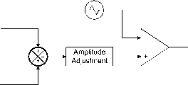 Another important element used in the control scheme is the filter that aUows us to generate p and q (Fig. 33.35). The frequency response of this filter is very important and must not introduce any phase-shift or attenuation to the low frequency harmonic components that must be compensated. A high-pass first order filter tuned at 15 Fiz is adequated. This corner frequency is required when single-phase nonlinear loads are compensated. In this case, the dominant current harmonic is the third. An example of the filter that can be used is shown in Fig. 33.37. The operator a required to calculate the sequence components of the system voltages (Fortescue transformation) can be obtained with the aU-pass filter shown in Fig. 33.38. The phase shift between Vq and is given by the foUowing expression: в = 2arctan(2/R2 0 (33.44) Since the phase-shift is negative, the operator a is obtained by using an inverter (180°) and then by tuning 9 = -60°. The operator a is obtained by phase-shifting Vl by -120°. Vl is synchronized with the system phase-to-neutral voltage yn-  ref FIGURE 33.37 The first-order high-pass fiher implemented for the calculation of p f and qf(C =€2 = 0.! /гЕ, = = 150 kQ, R2 = 50 kQ). Current Reference □ vo = vi /-0 FIGURE 33.36 The block diagram of the gating signals generator. FIGURE 33.38 The all-pass fiher used as a phase shifter. 33.4.6 Experimental Results The viabihty and effectiveness of series active power fihers used to compensate current harmonics was proved in an experimental setup of 5kVA. Current waveforms generated by a nonlinear load and using only passive filters and the combination of passive and the series active power filter are shown in Figs. 33.39 and 33.40. These figures show the effectiveness of the series active power filter, which reduces the overall THD of the current that flows through the power system from 28.9% (with the operation of only the passive filters) to 9% with the operation of the passive filters with the active power filter connected in series. The compensation of the current that flows through the neutral conductor is shown in Fig. 33.41.
СЫ 20.0mV
FIGURE 33.39 Experimental results without the operation of the series active power filter, (a) Load current, (b) Current flowing through the passive filter, (c) Current through the power supply. Ch4 20.0mv
nvMUUrnsi 5 Aug 199 17:26:2 (a) (b) (c) FIGURE 33.40 Experimental results with the operation of the series active power filter, (a) Load current, (b) Current flowing through the passive filter, (c) Current through the power supply. Ch4 SO.OmV 7 Aug 1997 16:31:22
FIGURE 33.41 Experimental results of neutral current compensation, (a) Current flowing through the neutral without the operation of the series active power filter, (b) Current flowing through the neutral with the operation of the active power filter. Acknowledgment The authors would like to acknowledge the financial support from FONDECYT through the 1990413 project. References 1. H. Akagi, Y. Kanzawa and A. Nabae (1984) Instantaneous reactive power compensators comprising switching devices without energy components. IEEE Trans. Ind. Appl, IA-20(3), 625-630. 2. S. Bhattacharaya and D. Divan (1995) Design and implementation of a hybrid series active filter system. IEEE Conference Record PESC 1995, pp. 189-195. 3. J. Dixon, S. Tepper and L. Moran (1996) Practical evaluation of different modulation techniques for current controlled voltage-source inverters, lEE Proc. on Electric Power Applications 143(4), 301-306. 4. A. Nabae, S. Ogasawara and H. Akagi (1986) A novel control scheme for current controlled PWM inverters, IEEE Trans, on Ind. Appl. lA-22(4), 312-323. 5. F. Z. Peng, H. Akagi and A. Nabae (1990) A new approach to harmonic compensation in power system-a combined system of shunt passive and series active filter, IEEE Trans, on Ind. Appl. IA-26 (Nov/Dec), 983-989. 6. R Z. Peng, M. Kohata, and H. Akagi (1993) Compensation characteristics of shunt passive and series active filters, IEEE Trans, on Ind. Appl. IA-29(1), 144-151. 7. T. Tanaka, K. Wada and H. Akagi (1995) A new control scheme of series active filters, Conference Record IPEC-95, pp. 376-381. 8. L. Moran, I. Pastorini, J. Dixon and R. Wallace (1999) A fauh protection scheme for series active power filters, IEEE Trans, on Power Electronics, 14(5), 928-938. 9. A. Campos, G. Joos, P. D. Ziogas and J. Lindsay (1994) Analysis and design of a series voltage unbalance compensator based on a three-phase VSI operating with unbalanced switching functions, IEEE Trans, on Power Electronics 9(3), 269-274. 10. G. Joos and L. Moran (1995) Principles of active power filters, IEEE- IAS 98 Tutorial Course Notes, October. 11. H. Akagi (1997) Control strategy and site selection of a shunt active filter for damping harmonics propagation in power distribution system, IEEE Trans, on Power Delivery 12(1), 17-28. 12. Hirofumi Akagi (1994) Trends in active power line conditioners, IEEE Trans, on Power Electronics 9(3), 263-268. 13. L. Moran, P. Ziogas and G. Coos (1993) A solid-state high performance reactive-power compensator, IEEE Trans, on Ind. Appl. 29(5), 969-978. 14. L. Moran, J. Dixon and R. Wallace (1995) A three-phase active power filter operating with fixed switching frequency for reactive power and current harmonic compensation, IEEE Trans, on Ind. Electronics 42(4), 402-408. 15. H. Fujita, S. Tominaga and H. Akagi (1996) Analysis and design of a dc voltage-controlled static var compensator using quad-series voltage-source inverters, IEEE Trans, on Ind. Appl. 32(4), 970-978. 16. V. Bhavaraju and P. Enjeti (1996) An active line conditioner to balance voltages in a three-phase system, IEEE Trans, on Ind. Appl. 32(2), 287-292. 17. Shoji Fukuda and Takayoshi Endoh (1995) Control method for a combined active filter system employing a current source converter and high pass fiher, IEEE Trans, on Ind. Appl. 31(3), 590-597. 18. T. Tanaka and H. Akagi (1995) A new method of harmonic power detection based on the instantaneous active power in three-phase circuit, IEEE Trans, on Power Delivery 10(4), 1737-1742. 19. Edson Watanabe, Richard Stephan and Mauricio Aredes (1993) New concepts of instantaneous active and reactive power in electrical system with generic loads, IEEE Trans, on Power Delivery 8(2), 697-703. 20. M. Aredes and E. Watanabe (1995) New control algorithms for series and shunt three-phase four-wire active power filter, IEEE Trans, on Power Delilvery 10(3), 1649-1656. 21. T. Tanaka, K. Wada and H. Akagi (1995) A new control scheme of series active filters, Conference Record IPEC-95, pp. 376-381. 22. T. Thomas, K. Haddad, G. Joos and A. Jaafari (1998) Design and performance of active power filters, IEEE Industry Applications Magazine 4(5), 38-46. 23. S. Bhattacharya, T. M. Frank, D. Divan and B. Banerjee (1998) Active filter implementation, IEEE Industry Applications Magazine 4(5), 47-63. 1 ... 82 83 84 85 86 87 88 ... 91 |
|||||||||||||||||||||||||||||||||||||||||||||||||||||||||||||||||||||||||||||||||||||||||||||||||||||||||||||||||||||||||||||||||||||||||||||||||||||||||||||||||||||||||||||||||||||||||||||||||||||||||||||||||||||||||||||||||||||||||||||||||||||||||||||||||||||||||||||||||||||||||||||||||||||||||||||||||||||||||||||||||||||||||||||||||||||||||||||||||||||||||||||||||||||||||||||||||||||||||||||||||||||||||||||||||||||||||||||||||||||||||||||||||||||||||||||||||||||||||||||||||||||||||||||||||||||||||||||||||||||||||||||||||||||||||||||||||||||||||||||||||||||||||||||||||||||||||||||||||||||||||||||||||||||||||||||||||||||||||||||||||||||||||||||||||||||||||||||||||||||||||||||||||||||||||||||||||||
|
© 2026 AutoElektrix.ru
Частичное копирование материалов разрешено при условии активной ссылки |