 |
 |
 |
| Главная Журналы Популярное Audi - почему их так назвали? Как появилась марка Bmw? Откуда появился Lexus? Достижения и устремления Mercedes-Benz Первые модели Chevrolet Электромобиль Nissan Leaf |
Главная » Журналы » Metal oxide semiconductor 1 ... 84 85 86 87 88 89 90 91 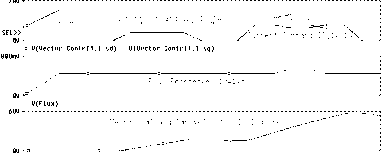 1 U(Omega nech) Os B.Us □ U(Motor1:Torque) * U(Torque) Torque & Torque Command e.8s 1.2s FIGURE 34.15 Results for indirect vector control with perfect tuning. SEL f CurrentCommand ID, 1У=1Й : U(Uector ContrI1.I sd) * U(Uector ContrI1.I sq) Flux- Reference, lV=lVs flechanical Angular Velocity, lV=lrad/sec : U(Onega nech)  Torque & Torque Command i O.iis 0.8s : U(Motor1:Torque) * U(Torque) Tine FIGURE 34.16 Results for indirect vector control with 125% rotor resistance. 34.6 Simulation of Sensorless Vector Control Using PSpice® Release 9 In the previous example, the advantages of vector control have been shown. Fiowever, for the implementation of the control scheme a sensor for the mechanical speed was necessary. This could pose a problem for applications, where a vector control unit is to be retrofitted into existing equipment. The motor instaUation may not easily aUow the instaUation of a mechanical speed sensor. Therefore engineers have thought to replace the mechanical speed sensor with a speed observer, which is a mathematical model that is evaluated by the control processor (typically a DSP), which is performing the standard vector control computations anyway. The algorithm for the observer would use the measured stator voltages and currents for the D and Q axis as input parameters. It would also rely on the knowledge of the machine model and on the correct machine parameters (rotor and stator resistance, mutual and leakage inductance, etc.). The following example shows such an arrangement. It could be derived from the previous example, with the only difference being that the speed sensor signal is replaced by a speed observer. Fiowever, careful examination of the derivation [3] of the speed observer reveals that it is easier to calculate the synchronous angular velocity, which is ultimately desired anyway, than the angular velocity of the rotor. Therefore, the observer was modified and the calculation of the rotor speed and the subsequent addition of the slip speed was foregone. The speed observer used here basically solves the D,Q equation system of the induction machine shown in Eqn. (34.3), with the only difference that some of the dependent variables are now independent and vice versa. In addition to the synchronous angular velocity, the observer provides the values of the rotor flux, which are used in the D axis signal path. The advantage of this is that the compensator with the differentiation function, which is problematic from a numerical stabihty standpoint, can be eliminated. Figure 34.17 shows the top level of a simulation project for sensorless vector control. This and the following figures for the sensorless control project show the screen view from PSpice® 9.0/ORCAD. The top view of this circuit is very similar to the circuit for the indirect vector control represented by Figs. 34.12 and 34.14 except for the missing motor-speed feedback. The model for the motor and the motors parameters are precisely the same as in the example for the indirect vector control. The circuit has originally been developed using MicroSims PSpice® 8.0 and subsequently imported into the PSpice® 9.0 environment using the File/Import Design... dialog. Selecting the Sensorless Vector Control block and choosing Descend Hierarchy reveals the associated subcircuit, which is shown in Fig. 34.18. This subcircuit is similar to the sub-circuit for the indirect vector control with two exceptions. First and foremost, the motor-speed feedback signal is replaced by the speed observer. In this case the speed observer directly provides the synchronous angular velocity. Therefore, it is not necessary to calculate the slip speed and add it to the FIGURE 34.17 Top level of simulation circuit for sensorless vector control. rotor speed to obtain the synchronous speed. Second, the values of the rotor flux, which are available from the speed observer, are used to calculate the reference value for the torque producing current (Q) component. Therefore, the compensation term, which contains a differentiator in the D axis of the controller shown in Fig. 34.13, can be ehminated. The purpose of the compensation term is to ensure that the flux is equal to the flux command at aU times with no delay. If that is assured, the command signal can be chosen in place of the real flux to calculate how much torque producing current is necessary to obtain the desired torque. Fiowever, if the actual flux is known (observed), this value can be used instead. Since the flux observer is fed by the D and Q axis voltages and currents for the stationary reference frame, the flux components need to be transformed back into the synchronous reference frame. This is done with the Negative Vector Rotator located above and to the left of the speed observer in Fig. 34.18. The PSpice® 9.0/ORCAD evaluation version has somewhat stricter hmitations for the number of graphical elements on the schematic pages of the project. Fiowever, the limitations for the number of nodes for the actual simulation engine are seemingly the same. Therefore, the extensive subcircuit of the induction motor model (see Fig. 34.9) has been replaced by a number of additional attributes, which have been added to the motor symbol using the symbol editor. The easiest way to start the symbol editor and to open the appropriate library is to select the symbol by clicking into it and then select the Edit Symbol function. The additional attributes of the modified motor symbol wiU enter the equivalent to the sub-circuit represented by Fig. 34.9 into the netlist. The nethst is a compilation of the schematic pages into a textual description in ASCII format. From a usability standpoint, a self contained symbol like this is a very elegant solution, since the file for the subcircuit is no longer required. Since the PSpice® simulation engine always uses the netlist as the input, the circuit works identically. For the PSpice® simulation it makes no difference where the netlist or part of it comes from. This also means that even the most recent release of PSpice® can stiU simulate legacy files that have been created before the introduction of schematic editors. The introduction of nethst entries is done via the TEMPLATE attribute. This attribute is a system attribute and a part of every symbol. Therefore, the TEMPLATE attribute is of course present in the attribute list for the motor symbols in the previous examples. These attribute lists are shown in Table 34.1 and 2. In these tables the TEMPLATE attribute has no value since the netlist entries are made by the symbols in the associated subcircuit. To give the reader a better understanding of the self-contained machine symbol, the format of some common nethst entries and the syntax of the value of the TEMPLATE attribute is now discussed. It is also very helpful to examine the TEMPLATE attributes of existing symbols. The format of the netlist entries for some common elements is ([] denotes space holder for name extension specific for a symbol to avoid duplicate names): Resistors (R devices) Generic: Rname [] Example: Rsd[] Example: Rsd[] Example: Rsd[] --Node[] - Node[] Value ;Optional Comment Rsd-b[] Rsd-[] Rsd-b[] Rsd-[] %D 0 1.0k {@Rs} 1.0k ;Resistor, fixed Value ;Resistor, Value Rs passed on ;Resistor, Ik, Pin D to Gnd Inductors (L devices): Generic: Lname[] --Node[] -Node[] Value ;Optional Comment Example: Lsd[] Lsd-b[] Lsd-[] l.Ou ;Inductor, l.O/H fixed Example: Lsd[] Lsd-b[] Lsd-[] {@Lsl} ;Inductor, Value Lsl passed on Voltage-controlled voltage sources (E devices) Generic: Ename[] -bOut[] -Out[] VALUE { Control Function } Example: ETorque[] %Torque 0 VALUE { 1.5*(Vtl[] - Vt2[]) } ;E source, output between pin Torque and Gnd, Control fianction as shown Figure 34.19 shows the screen view of the symbol for the induction motor in the symbol editor in PSpice® Release 8.0, which was used for the development of this part. Figure 34.20 shows a similar view; however, here the window for entry and editing of attributes is also visible. This screen can be invoked using the Part/Attributes... dialog. The attributes that create the netlist entries, which insert the previously discussed model for the motor, are entered here. A complete hst of aU attributes, extracted from a working example, is given in Table 34.3. Therefore, the reader should be able to enter the attributes exactly as printed and obtain a working model, which can be used in PSpice® Release 8.0 and 9.0. According to Table 34.3, the value for the TEMPLATE attribute is as foUows: TEMPLATE = @ElectricD\n\n@ElectricQ\n\n@Mechanical This statement wiU insert the expression for ElectricD , i.e. the T-equivalent circuit for the D axis, two carriage returns \n\n , the expression for ElectricQ , i.e. the T-equivalent circuit for the Q axis, two more carriage returns \n\n , and finally the expression for Mechanical , i.e. the mechanical model into the nethst. The expressions for ElectricD , ElectricQ , and Mechanical are defined in separate attributes. Careful examination of the values of the ElectricD , ElectricQ , and Mechanical attributes reveals a number of FIGURE 34.20 Screen view of symbol editor with attribute input window. FIGURE 34.19 Screen view of motor symbol in the symbol editor. TABLE 34.3 List of all attributes used for the self-contained induction motor symbol Attributes REFDES = Motor? PART = Ind Motor MODEL = Ind Motor TEMPLATE = @ElectricD\n\n@ElectricQ\n\n@Mechanical R Stat = 0.48 R Rot = 0.358 Lm = 51.25mH Lsl = 2.18mH Lrl = 2.89mH J mot = 0.1 Omega init = 0.0 Poles = 4 ElectricD = Rsd@REFDES %D 1@REFDES @R Stat \nLsld@REFDES 1@REFDES Vmd@REFDES @Lsl \nLmd@REFDES Vmd@REFDES 0 @Lm \nLrld@REFDES Vmd@REFDES 2@REFDES @Lrl \nRrd@REFDES 2@REFDES ErotD@REFDES @R Rot \nErotd@REFDES ErotD@REFDES 0 VALUE {-(Ome@REFDES)*((V(%Q,3@REFDES)/@R Stat)*@Lm \n + + (V(ErotQ@REFDES,4@REFDES)/@R Rot)*(@Lm + @Lrl)) } ElectricQ = Rsq@REFDES %Q 3@REFDES @R Stat \nLslq@REFDES 3@REFDES Vmq@REFDES @Lsl \nLmq@REFDES Vmq@REFDES 0 @Lm \nLrlq@REFDES Vmq@REFDES 4@REFDES @Lrl \nRrq@REFDES 4@REFDES ErotQ@REFDES @R Rot \nErotq@REFDES ErotQ@REFDES 0 VALUE {V(Ome@REFDES)*((V(%D,l@REFDES)/@R Stat)*@Lm \n + + (V(ErotD@REFDES,2@REFDES)/@R Rot)*(@Lm + @Lrl)) } Mechanical = ETorque@REFDES %Torque 0 \n + VALUE { (L5*@Lm*@Poles/2) * ( \n + ((V(%Q,3@REFDES)/@R Stat)*(V(ErotD@REFDES,2@REFDES)/@R Rot)) -\n + ((V(%D,l@REFDES)/@R Stat)*(V(ErotQ@REFDES,4@REFDES)/@R Rot)) ) } \nEOme@REFDES Ome@REFDES 0 VALUE {V(Om@REFDES)*@Poles/2 } \nVLd@REFDES Om@REFDES %Omech OV \nEom@REFDES Om@REFDES 0 VALUE {SDT(( V(%Torque)-I(VLd@REFDES) )/@J mot) + @Omega init } repetitive terms. The meaning of these terms are explained below: @Name Substitutes what is defined for @Name at the current place. @REFDES Inserts the path and the reference designator @REFDES to create a unique node or part name, that does not repeat. The path is the concatenation of the names of the symbols and sub-circuits in the hierarchy above the part. The reference designator is the name of the part on a particular schematic page. \n new hne (carriage return) is inserted into the netlist; however the value of the attribute does not have a carriage return in it. This means everything hsted after ElectricD until ElectricQ goes on one line. If the symbol definition is printed however, it is shown as in Table 34.3. \n+ new line and continuation of expression. \n + + new line, continuation of expression, numerical operator + . Figure 34.21 shows a subcircuit for the speed observer. This schematic shows the structure and aU the details of the implementation in the form of a block diagram. The speed observer uses the stator voltages and currents for the D and the Q axis as input variables. After subtracting the voltage drop across the winding resistance and the leakage inductance of the stator from the stator input voltage and scaling the result by Тг/Тщ the observer calculates the D and Q components of the rotor flux by integration. Since the input values are in the stationary reference frame, so are the results. The observer also calculates the magnitude of the rotor flux and then calculates the synchronous angular velocity by evaluating the rate of change of the ratio of the D and Q components. The mathematical relationships are given by Eqns. 34.9 and 34.10 [3]: R, + (jLP 0 0 + (tLp
cr = - atan -i- (LA)} g = leakage factor (34.9) = Ш = 4q(tMrd(t)-Arq(t)Ard(t) (rd(tr+rq(t)) (34.10) Since the observer shown in Fig. 34.21 has a large number of elements, this sub-circuit has also been integrated into a custom part by creating an appropriate TEMPLATE and other supporting attributes. A complete hsting, which was extracted from thoroughly tested part, is given in Table 34.4. Using this table, the reader should be able to create this very complex part with relative ease. Figure 34.22 shows the output for the sensorless vector control project as it presents itself in the PSpice® 9.0/ORCAD evaluation version. A comparison of the traces for the torque and the torque command (they are perfectly on top of each other) shows that FIGURE 34.21 Subcircuit for speed observer for sensorless vector controller. TABLE 34.4 List of all attributes for the speed observer symbol Attributes REFDES = Speed Observer? PART = Speed Obs MODEL = Speed Obs TEMPLATE = Ed@REFDES %Psi d 0 VALUE { @EXP dl \n+ @EXP d2 \n+ @EXP d3 } \nEq@REFDES %Psi q 0 VALUE { @EXP ql \n+ @EXP q2 \n+ @EXP q3 } \nEmag@REFDES %Psi mag 0 VALUE { V(%Psi d)*V(%Psi d)+ V(%Psi q)*V(%Psi q) } \nExr@REFDES %Psi xr 0 VALUE { @EXP xl \n+ @EXP x2 \n+ @EXP x3 \n+ @EXP x4 } \nEOmSync@REFDES %OmSync 0 VALUE { @EXP oml } SIMULATIONONLY = EXP dl = @Ini d + EXP d2 = SDT( (@Lr/@Lm)*( V(%V d) - V(%I sd)*@R Stat EXP d3 = -DDT(V(%I sd))*@Ls*@Sigma ) ) EXP ql = @Ini q + EXP q2 = SDT( (@Lr/@Lm)*( V(%V q) - V(%I sq)*@R Stat EXP q3 = -DDT(V(%I sq))*@Ls*@Sigma ) ) Ini d = O.OV Ini q = O.OV EXP xl = ( V(%Psi d)*(@Lr/@Lm)* EXP x2 = ( V(%V q) - V(%I sq)*@R Stat - DDT(V(%I sq))*@Ls*@Sigma ) ) EXP x3 = -( V(%Psi q)*(@Lr/@Lm)* EXP x4 = ( V(%V d) - V(%I sd)*@R Stat - DDT(V(%I sd))*@Ls*@Sigma ) ) EXP oml = ( V(%Psi xr)/(V(%Psi mag)+ lu) ) FIGURE 34.22 Simulation results for sensorless vector control. the scheme works perfectly. It even works for a start from zero speed, which is typically not the case in real systems. The reason is, that the uncertainties of the winding resistance values (note that they change with temperature) create errors in observers like this one. The problem is worst at low speeds, because at low speeds and associated low stator frequencies, the uncertain winding resistance represents a large part of the total machine impedance. It should be acknowledged at this point, that these examples have been created by Ali Ricardo Buendia, who is presently working towards his MSEE degree. The advantages of Simplorer® are that it has a lot of models for power electronics devices and machines built in, since it is specialized for this type of simulation. Also, no numerical convergence problems have been noticed thus far. Figure 34.23 shows the schematic for a three-phase diode rectifier. The input is a balanced three-phase source with a reactive source impedance. An exponential characteristic, closely resembling real diodes, has been chosen as a model for the diodes. Figure 34.24 shows a circuit which transforms the load currents from a three-phase to a two-phase system. Here the D, Q components are called alpha, beta components. The 34.7 Simulations Using Simplorer® In the following, some examples of simulations with the evaluation version of Simplorer® [9], Release 4.1 are shown. results of the simulation are shown on the same page that is used for the schematic diagrams shown by the previous two figures. Figure 34.25 shows a plot of the line currents during the start-up of the rectifier, where the initial load current is zero. The next graph shows a plot of the line currents that have been transformed by the circuit shown in Fig. 34.24. The components of the hne currents are the variables of the axes. The plot shows the typical hexagonal trace that can be expected for this type of line commutated rectifier (six-step operation). If the converted source voltages were plotted in this fashion, a perfect circle would be the result. The last two graphs demonstrate a Simplorer® simulation of the start of an induction motor. As previously mentioned, the symbol and the model for the induction motor is built into the code. Figure 34.27 shows the schematic with the source and the induction motor as weU as a graph that shows the rotational speed as a function of time. The graph below shows plots of the stator and rotor flux components, which are available from the machine model. Like the plot of the current components for the rectifier, the flux components are the variables of the axes in the graphs of Fig. 34.28. FIGURE 34.26 rectifier. Plot of converted load currents for the three-phase FIGURE 34.24 Three-phase to two-phase conversion for load currents. FIGURE 34.27 Simplorer® schematics for induction motor start. FIGURE 34.25 Simplorer® plot of load currents for the three-phase rectifier. FIGURE 34.28 Simplorer® plots of machine fluxes for induction motor start. 34.8 Conclusions In this chapter, the capabihties of two versions of PSpice® [12] and a version of Simplorer® [9] have been used to simulate a number of projects from the power electronics, machines and drives area. The advantage of PSpice® is that it is based on the almost universal Spice simulation language, which can be seen as the worldwide de facto standard. On the other hand Simplorer® has the advantage of built-in machine models. If both programs are used, comparisons and mutual vahdations of models can be performed. The reader should always validate any model before it is used for critical engineering decisions. It was pointed out in the introduction, that model validation often means verification that the hmitations of the model are not exceeded. In addition to the detailed examples, some general guidelines on the uses of simulation for analysis and design have been developed. All tested programs yielded excellent results. The simulation time for each project shown is typically less than a minute on a 400 MHz PC. It is hoped that the reader has obtained an insight and appreciation of the power of these modern simulation codes and some useful ideas and inspirations for projects of his own. References 1. Michael G. Giesselmann (1997) Averaged and cycle by cycle switching models for Buck, Boost, Buck-Boost and Cuk converters with common average switch model. Proceedings of the 32nd Intersociety Energy Conversion Engineering Conference, IECEC-97, Honolulu, HI, July 27-Aug 01, 1997. 2. Ned Mohan, Tore Undeland and WiUiam Robbins (1995) Power Electronics, Converters, Applications, and Design, 2nd edn, John Wiley & Sons, New York. 3. Andrzej M. Trzynadlowski (1994) The Field Orientation Principle in Control of Induction Motors, Kluwer, Amsterdam. 4. Donald W. Novotny, and Tom A. Lipo (1996) Vector Control and Dynamics of AC Drives. Oxford Science Publications, Oxford. 5. Peter Vas (1990) Vector Control of AC Machines. Oxford Science Publications, Oxford. 6. K. Hasse (1969) Zur Dynamik Drehzahlgeregelter Antriebe mit Stromrichter gespeisten Asynchron-Kurzschlusslaufermachinen (On the Dynamics of Adjustable Speed Drives with converter-fed Squirrel Cage Induction Machines). Ph. dissertation. Technical University of Darmstadt. 7. Paul C. Krause, Oleg Wasynczuk and Scott D. Sudhoff (1995) Analysis of Electric Machinery. IEEE Press, New York. 8. Annette Von Jouanne, D. Rendusara, P. Enjeti and W. Gray (1996) Filtering Techniques to minimize the effect of long motor leads on PWM inverter fed ac motor drive systems, IEEE Transactions on Ind. Applications, July/Aug., 919-926. 9. Simplorer®. Technical Documentation, SIMEC Corp., 1223 Peoples Avenue, Troy, NY 12180, USA, Info@Simplorer.com. 10. M. Giesselmann (1999) A PSpice® tutorial for demonstrating digital logic. IEEE Transactions on Education, Nov. 1999, http: coeweh. engr. unr. edu/eee/59/CDROM/Begin.htm. 11. ADMC-200 Data Sheet Analog Devices, Analog Devices, Inc., Corporate Headquarters, Building Three, Three Technology Way, Norwood, MA, USA, http:/ / products, analog, com/procucts/ info, aspfproduct = ADMC200. 12. PSpice® Documentation. 555 River Oaks Parkway, San Jose, CA 95134, USA, http: pcb.cadence.com/. Packaging and Smart Power Systems Douglas C. Hopkins, Ph.D Energy Systems Institute State University of New York at Buffalo Room 312, Bonner Hall Buffalo, New York 14260-1900, USA 35.1 35.2 35.3 35.4 35.5 35.6 35.7 Introduction...................................................................................... 871 Background....................................................................................... 871 Functional Integration......................................................................... 872 35.3.1 Setting User Requirements 35.3.2 Steps To Partitioning Assessing Partitioning Technologies....................................................... 874 35.4.1 Levels of Packaging 35.4.2 Technologies 35.4.3 Semiconductor Power Integrated Circuits FuU-Cost Model [5]............................................................................ 877 Partitioning Approach......................................................................... 879 Example 2.2 kW Motor Drive Design..................................................... 880 35.7.1 User Requirements (constraints) 35.7.2 Component Characterization Map 35.7.3 Component Grouping 35.7.4 Strategic Partitioning with Constraints 35.7.5 Optimization within Partitions References.......................................................................................... 882 35.1 Introduction A continual endeavor in power electronics is to increase power density. This is achieved by shrinking component size, moving components closer and reducing component count. During the last two decades circuit frequencies increased sharply to shrink component dimensions. Improved thermal management and physical packaging materials brought components closer. And finally, increased integration of functions at the semiconductor and package levels reduced component count. This has been marked in the microelectronics world by system on chip (SOC) and system on package (SOP), aU addressing higher densities and aU applicable to power electronic systems. The latter approach of functional integration has been ongoing for decades. Until the 1980s nearly aU such integration was done at the packaging level melding control and power processing. The term smart power (within the context of power electronic conditioning) apphed in the 1960s-1970s to the integration of computers and microprocessors into large rectifier and converter cabinets. With the advent of high-voltage-silicon integrated circuits more functionality was brought directly to the power semiconductors, and in the 1980s-1990s the term applied mostly to smart power semiconductors. In the late 1990s there was a move back to hybrid integration following the trend to SOP. The term Smart Power has also been commercially associated with power management circuits. From a designers perspective, functional integration exists in a packaging continuum with smart power as a subset, dependent on the definition in vogue. To take advantage of functional integration the designer, in reverse thinking, partitions or modularizes circuits and functions to achieve the most cost-effective approach that meets a set of required performance specifications. This chapter provides background information, framework and procedures to produce partitioning and functional integration. 35.2 Background Circuits are typically designed with a pre-determined idea of what packaging technologies wiU be used. The technologies range from sihcon integration of subcircuit functions to multiple boards in a rack. Partitioning a circuit packaged in one technology, such as aU silicon, is straightforward. Partitioning a circuit in multiple technologies is much more difficult since higher performing technologies duplicate aspects of lower technologies. The duplication geometrically increases parameter trade-offs and causes wasted packaging cost. Considerable literature exists about the technical characteristics of packaging materials and processes. (A table of characteristics is provided later.) Also, a study on the Status on Power Electronics Packaging (STATPEP) [1] identifies metrics to further evaluate the relative technical merits. To optimize the use of multiple technologies in functional integration, a structured method should be used. A full-cost model for various technologies is used as a basis to produce a comparative cost diagram. The diagram allows intermixing of high and low performance technologies based on surface density, which is interpreted as circuit area and, hence, a partition. An example is given in Section 35.7 to demonstrate the method using a 2.2 kW motor drive module product. The method is also applied to product modularization, i.e. system partitioning where a specific function is used across several products. A module can represent functional integration within a packaging technology or use multiple packaging technologies to create integrated power modules (IPMs) or power electronic building blocks (PEBBs). The importance of modularization is to increase product volume to lower cost. The cost model includes variations based on volume. This partitioning approach matches user requirements to Levels of Packaging as defined in the Framework for Power Electronics Packaging [2] and provides optimum integration of packaging levels for a product. The Framework also identifies critical technical issues that need to be considered in evaluating technical performance. This partitioning approach looks at electrical, magnetic, thermal and mechanical issues (multiple energy forms). 35.3 Functional Integration Figure 35.1 shows a 2.2 kW ac motor drive. Functional integration requires that the system be partitioned both electrically and physically. The systems integrator is usually an electrical designer and the first partitioning is usually electrical. The electrical partitions and distributed power losses are also shown in the figure. The physical partitioning, or packaging, involves different components with different functions ranging from fine-hne control to high-current, high-loss power processing. Several partitions can be pursued. The Line-communications and Motor-control Blocks can use a signal-level packaging approach, such as all-silicon ASIC (application-specific integrated circuit), or discrete components on an epoxy-glass (FR-4) or insulated-metal substrates (IMS). If the Power Supply and Control Blocks are to be combined, an SMT approach cannot accommodate bulky storage components in the power supply. Hence, a through-hole approach is considered for part or both blocks. Regardless, such tradeoffs can be nearly endless. A structured method needs to be used to establish essential requirements and guide circuit and system partitioning. The method described here is based on characterizing and grouping the components, eval- Leaded (outside D die T (inside the dotted box) the dotted ox) 1 coil 10W 10 XXpulse -caps 3 VDR 1 Resistor
ecti ier communication о er su I
A С ine CO nication о er s ply 1 Transformer 4 Capacitors 12 D 3 D 3 esistors FIGURE 35.1 Block diagram of a 2.2 kW motor drive module. Reprinted with permission, JB Jacobsen and DC Hopkins, Optimally selecting packaging technologies and circuit partitions based on cost and performance. Applied Power Electronics Conference, New Orleans, LA, February 6-10 2000, ©2000, IEEE, New York. 1 ... 84 85 86 87 88 89 90 91 |
|||||||||||||||||||||||||||||||||||||||||||||||||||||||||||||||||||||||||||||||||||||
|
© 2026 AutoElektrix.ru
Частичное копирование материалов разрешено при условии активной ссылки |