 |
 |
 |
| Главная Журналы Популярное Audi - почему их так назвали? Как появилась марка Bmw? Откуда появился Lexus? Достижения и устремления Mercedes-Benz Первые модели Chevrolet Электромобиль Nissan Leaf |
Главная » Журналы » Metal oxide semiconductor 1 ... 6 7 8 9 10 11 12 ... 91 of device structure, geometry, and bias voltages. During turn-on, capacitors Cgj and Cg must be charged through the gate, hence, the design of the gate control circuit must take into consideration the variation in these capacitances. The largest variation occurs in the gate-to-drain capacitance as the drain-to-gate voltage varies. The MOSFET parasitic capacitance is given in terms of the device data sheet parameters Qg, Qsg, and as follows: gd - Qss gs - Qss ~ Qss Qs - Qss ~ Qss where is the small-signal reverse transfer capacitance; Qg is the small-signal input capacitance with the drain and source terminals shorted; and C is the small-signal output capacitance with the gate and source terminals shorted. The MOSFET capacitances Cg, Cgj and are nonlinear and a function of the dc bias voltage. The variations in C and are significant as the drain-to-source voltage and the gate-to-source voltage each cross zero. The objective of the drive circuit is to charge and discharge the gate-to-source and gate-to-drain parasitic capacitances to turn on and off the device, respectively. 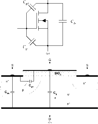 In power electronics, the aim is to use power-switching devices that operate at higher and higher frequencies. Fience, the size and weight of output transformers, inductors, and filter capacitors will decrease. As a result, MOSFETs are now used extensively in power supply design that requires high switching frequencies, including switching and resonant mode power supplies and brushless dc motor drives. Because of its large conduction losses, its power rating is limited to a few kilowatts. Because of its many advantages over BJT devices, modern MOSFET devices have received high market acceptance. 6.6 MOSFET Regions of Operation Most MOSFET devices used in power electronics applications are of the n-channel, enhancement type, like that shown in Fig. 6.6a. For the MOSFET to carry drain current, a channel between the drain and the source must be created. This occurs when the gate-to-source voltage exceeds the device threshold voltage Vj. For Vq > Vj, the device can be either in the triode region, which is also called constant resistance region, or in the saturation region, depending on the value of is-given Vq, with small is (ds < gs ~ Th) the device operates in the triode region (saturation region in the BJT), and for larger Vy)s (ds > gs ~ Th) the device enters the saturation region (active region in the BJT). For Vq < У^, the device turns off, with drain current almost equal to zero. Under both regions of operation, the gate current is almost zero. This is why the MOSFET is known as a voltage-driven device and, therefore, requires simple gate control circuit. The characteristic curves in Fig. 6.6b show that there are three distinct regions of operation labeled as triode region, saturation region, and cut-off region. When used as a switching device, only triode and cut-off regions are used, whereas, when it is used as an amplifier, the MOSFET must operate in the saturation region, which corresponds to the active region in the BJT. The device operates in the cut-off region (off-state) when gs < Th resulting in no induced channel. In order to operate the MOSFET in either the triode or saturation region, a channel must first be induced. This can be accomplished by applying gate-to-source voltage that exceeds Vj, that is. FIGURE 6.9 (a) Equivalent MOSFET representation including junction capacitances; and (b) representation of this physical location. Once the channel is induced, the MOSFET can operate in either the triode region (when the channel is continuous with no pinch-off, resulting in drain current proportional to the channel resistance) or the saturation region (the channel pinches off, resulting in constant Ij). The gate-to-drain bias voltage (vqy)) determines whether the induced channel enters pinch-off or not. This is subject to the following restriction. For a triode mode of operation, we have GD > Th GD < УТЪ And for the saturation region of operation, pinch-off occurs when Vqj) = Vrh- In terms i;j)S the preceding inequahties may be expressed as foUows. 1. For triode region of operation DS < GS - Th and > Vrh 2. For saturation region of operation DS > GS - Th and > Vrh 3. For cut-off region of operation (6.3) (6.4) (6.5) It can be shown that drain current ip, can be mathematicaUy approximated as follows: in = K[2(vqs - VTh)tDS - Ds] triode region (6.6) ip) = K(vq - yh) saturation region (6.7) where and is the electron mobility; Cqx is the oxide capacitance per unit area; L is the length of the channel; and W is the width of the channel. Typical values for these parameters are given in the PSpice model that wiU be discussed later. At the boundary between the saturation (active) and triode regions, we have DS - GS ~ 1 which results in the foUowing equation for ip,: (6.8) (6.9) The input transfer characteristics curve for i vs Vq is when the device is operating in the saturation region shown in Fig. 6.10. The large signal equivalent circuit model for an n-channel enhancement-type MOSFET operating in the saturation mode is shown in Fig. 6.11. The drain current is represented by a current source as the function of Vh and Vq. figure 6.10 Input transfer characteristics for a MOSFET device when operating in the saturation region.  figure 6.11 Large signal equivalent circuit model. If after the channel is pinched-off, we assume that the drain-source current wiU no longer be constant but rather depends on the value of is as shown in Fig. 6.12, then the increased value of Vj) cause a reduced channel length, resulting in a phenomenon known as channel-length modulation [3, 4]. If the i;j)s ~ Ь lis are extended as shown in Fig. 6.12, they aU intercept the v-axis at a single point labeled - 1/Я, where Я is  Increasing figure 6.12 The MOSFET characteristics curve including output resistance. a positive constant MOSFET parameter. The term (1 + Ais) is added to the ij equation in order to account for the increase in ij due to the channel-length modulation. Fiere ij is given by ij = k(vQ - VTh)(l + Ds) saturation region (6.10) From the definition of the Tq given in Eq. 6.11, it is easy to show that the MOSFET output resistance can be expressed as follows: (6.11) If we assume that the MOSFET is operating under small signal condition, that is, the variation in Vq on ij vs Vq is in the neighborhood of the dc operating point Q at ij) and Vq as shown in Fig. 6.13. As a result, the i, current source can be represented by the product of the slope g and Vq as shown in Fig. 6.14. Slope=g m 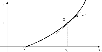 FIGURE 6.13 Linearized z, vs Vq curve with operating dc point (g).  FIGURE 6.14 Small signal equivalent circuit including MOSFET output resistance. 6.6.1 MOSFET Switching Characteristics Because the MOSFET is a majority carrier transport device, it is inherently capable of high frequency operation [5-8]. Fiowever, the MOSFET has two hmitations: 1. high input gate capacitances; and 2. transient/delay due to carrier transport through the drift region. As stated earlier, the input capacitance consists of two components: the gate-to-source and gate-to-drain capacitances. The input capacitances can be expressed in terms of the device junction capacitances by applying the Miller theorem to Fig. 6.15a. Using the Miller theorem, the total input capacitance Qj, seen between the gate-to source, is given by Qn = Cgs + (i+ii)Cgd (6.12) The frequency responses of the MOSFET circuit are hmited by the charging and discharging times of Q. The Miller effect is inherent in any feedback transistor circuit with resistive load that exhibits a feedback capacitance from the input and output. The objective is to reduce the feedback gate-to-drain resistance. The output capacitance between the drain-to-source Qs does not affect the turn-on and turn-off MOSFET switching characteristics. Figure 6.16 shows how Cgj and Cgs vary under increased drain-source is voltage. In power electronics apphcations, power MOSFET are operated at high frequencies in order to reduce the size of 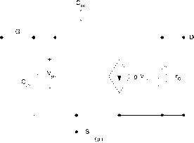 FIGURE 6.15 (a) Small signal model including parasitic capacitances, (b) Equivalent circuit using Miller theorem. Capacitance 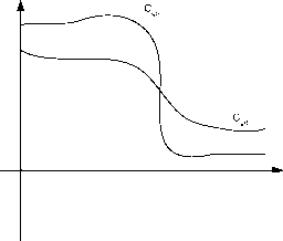 Voltage FIGURE 6.16 Variation of Cgj and Cg as a function of Vj. the magnetic components. In order to reduce the switching losses, power MOSFET are maintained in either the on-state (conduction state) or the off-state (forward-blocking) state. It is important we understand internal device behavior, which leads to an understanind of the parameters that govern the device transition from the on-state and off-states. To investigate the on- and off-switching characteristics, we consider the simple power electronic circuit shown in Fig. 6.17a under inductive load. The flyback diode D is used to pick up the load current when the switch is off. To simplify the analysis we wiU assume the load inductance is a large enough Lq that the current through it is constant as shown in Fig. 6.17b. 6.6.2 Turn-On Characteristics Let us assume initially that the device is off and that the load current Iq, flows through D as shown in Fig. 6.18a, Vqq = 0. The voltage is = dd and Iq = ij)- At t = tg, the voltage Vqq is applied as shown in Fig. 6.19a. The voltage across Cs starts charging through Rq. The gate-source voltage, Vq controls the flow of the drain-to-source current i,. Let us assume that for to < t < tj, Vq < Vj, that is, the MOSFET remains in the cut-off region with ip, = 0, regardless of is- The time interval (21, to) represents the delay turn-on time needed to change C(3s from zero to У^. The expression for the time interval AtiQ = tj - to can be obtained as shown next. The gate current is given by (6.13) GS GS 4 G - Vb) ~ -GD О 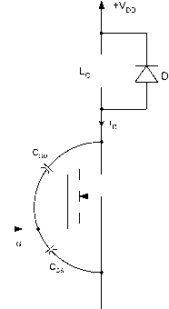 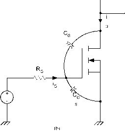 FIGURE 6.17 (a) Simplified equivalent circuit used to study turn-on and turn-off characteristics of the MOSFET; and (b) simplified equivalent circuit. then Iq is given by wliere Vq and are gate-to-ground and drain-to-ground voltages, respectively. As we have Vq = Vq, = +v[3d> GS + cgd) (6.14) 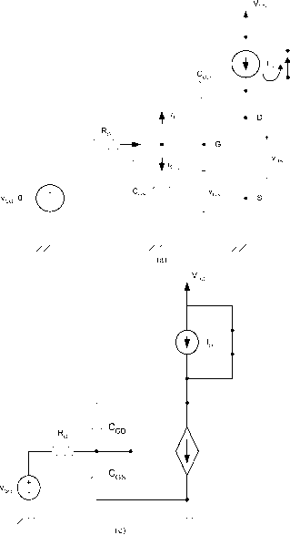 о iG=0 R. G FIGURE 6.18 Equivalent modes: (a) MOSFET is in the off-state for t < t, Vqq = 0, Vjs = dd> h = 0 = 0; (b) MOSFET is in the off-state with GS < Th for h> (c) > Th> h < h for 1 < < 2; (d) igs > Th> = for h<t < h and (e) Uqs > xh. 0 =ht> h the device is fully on. From Eqs. (13) and (14), we obtain, . GG ~ GS = (Cgs + Qd) (6.15) Solving Eq. (6.15) for %s(0 for t > t with %s(o) = 0 obtain. where %s(0 = gg(1 - e~l - g(gs + gd) (6.16) The gate current is given by GG ~ iGS J- =le-(t-to)/T Rg (6.17) As long as tJQs < Th> d remains zero. At f - fp reaches Vjh, causing the MOSFET to start conducting. Waveforms for ig and are shown in Fig. 6.19. The time interval (fj - t) is given by Atio = = -Tin 1 - AtiQ represents the first delay interval in the turn-on process. For t > tl with Vq > yh the device starts conducting and its drain current is given as a function of Vq and У^. In fact, ip) starts flowing exponentially from zero as shown in Fig. 6.19d. Assume the input transfer characteristics for the MOSFET are limited as shown in Fig. 6.20 with the slope of gm given by 2y bssh (6.18) The drain current can be approximated as foUows: d(0 = >gs - Th) (6.19) As long as ip)(t) < Iq, D remains on and is = dd shown in Fig. 6.18c. The equation for igs(0 remains the same as in Eq. (6.16), hence, Eq. (6.19) results in ip)(t) given by (6.20) The gate current continues to decrease exponentially as shown in Fig. 6.19. At t = i) reaches its maximum value of Iq, turning D off. The time interval At2i = (2 - t) is obtained from Eq. (20) by setting i]:,(t2) = Iq. А^21 = Tin GG-Th)- (6.21) 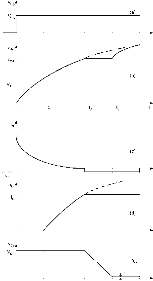 t t t t time FIGURE 6.19 Turn-on waveform switching. For t > t2 the diode turns off and ij) Iq is as shown in Fig. 6.18d. As the drain-current is nearly a constant, then the gate-source voltage is also constant according to the input transfer characteristic of the MOSFET, that is. Ь = gmigs - Th) Iq (6.22) Hence, %s(0 = -+Th (6.23) dc operating point 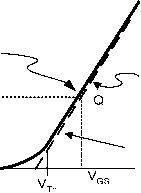 Slope=gm ideal FIGURE 6.20 Input transfer characteristics. At t = icit) is given by Т/ и л gg - - Th gg - GSKh) gm (6.24) As the time constant т is very small, it is safe to assume that Gs(2) reaches its maximum, that is. %s(2) GG For t2 < t < the diode turns off the load current Iq and (drain current ij) starts discharging the drain-to-source capacitance. As Vq is constant, the entire gate current flows through Cqy), which results in the following relation. - It With Vq constant and = 0, we have Solving for iDs(0 for t > with 105(2) = dd obtain Ds(0 = - ~ (t - h) + Vdd for t > t2 (6.25) This is a linear discharge of С^ as shown in Fig. 6.19e. The time interval А%2 = (% - 2) is determined by assuming that at t = %, the drain-to-source voltage reaches its minimum value determined by its on-resistance, ids(on) that is, vs(o) is given by ds(on) ds(0]v) = constant For t > the gate current continues to charge rid as vs is constant, Vq starts charging at the same rate as in interval tQ < t < tj, that is, %s(0 = Vgg(1 - e--/) The gate voltage continues to increase exponentially until t = %, when it reaches Vqq, at which Iq = 0 and the device fully turns on as shown in Fig. 6.18e. We have equivalent circuit model when the MOSFET is completely turned on for t > t. At this time, capacitors Cq and are charged with Vqq and (/оГо8(ом) - gg) respectively. The time interval А%2 = (% - 2) is obtained by evaluating v at t = % as follows: М^з) = -%7Т^(%-2)+00 = ods(on) Fience, А^з2 = (% - 2) is given by At -t t-ur (dd -ds(on)) gg - Th The total delay in turning on the MOSFET is given by = Atio + at2i + А%2 (6.28) (6.26) (6.27) Notice that the MOSFET sustains high vohage and current simuhaneously during intervals At2i and А%2. This results in large power dissipation during turn-on, which contributes to overaU switching losses. The smaller the Rq, the smaUer At2i and А%2 become. 6.6.3 Turn-off Characteristics To study the turn-off characteristic of the MOSFET, we will consider Fig. 6.17b again by assuming the MOSFET is on and in steady state at t > tg with the equivalent circuit of Fig. 6.18(e). Therefore, at t = we have the following initial conditions:
(6.29) At t = to, the gate voltage igg(0 is reduced to zero as shown in Fig. 6.21a. The equivalent circuit at t > tg is shown in Fig. 6.22a. We assume that the drain-to-source remains constant while C(3s and C(3d are discharging through Rq as governed by the foUowing relations. 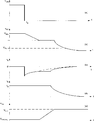 to tl *2 *3 V FIGURE 6.21 Turn-on switching waveforms. - Cos + Cgd As Vy)s is assumed constant, then Iq becomes = (Cgs + Cgd)- Hence, evaluating for Vq for t > tg, we obtain Where (6.30) (6.31) %s(o) = %g - (gs + gd)g As Vq continues to decrease exponentially, drawing current from Cqy), it wiU reach a constant value at which drain current is fixed, that is, Ip, = Iq. From the input transfer characteristics, the value of Vq, at which 1, = Iq, is given by 0 , ТГ gs = - + Th (6.32) The time interval At = h ~ h t)e obtained easily by setting Eq. (6.31) to Eq. (6.32) at t= tj. The gate current during the t2 < t < t is given by (6.33) Because for t2 - t the gate-to-source voltage is constant and equals %s(i = o/Sm + Th s shown in Fig. 6.21b, then the entire gate current is being drawn from С^ and Iq = C( d(vgs - ds) dds - -gd 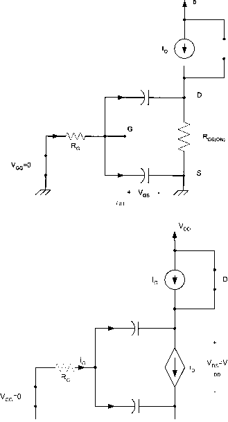 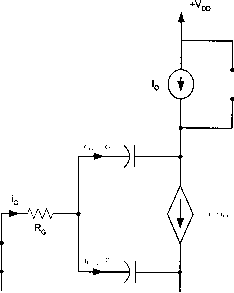 ra/w + VGS = i+V 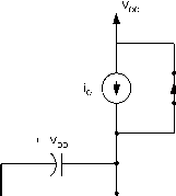 (c) (d) FIGURE 6.22 Equivalent circuits: (a) < < i; (b) < < (c) t2 < t < ty, and (d) < t < t. Assuming Iq constant at its initial value at t = t, that is, At t = the drain-to-source voltage becomes equal to yj)D forcing D to turn-on as shown in Fig. 6.22c. The drain-to-source current is obtained from the transfer - -- - - I--h Rn Rr g \6m characteristics and given by Integrating both sides of the preceding equation from to t i (t) - cr (v - V ) With idsci) = -DS(ON) we obtam I / J \ Where igs(0 is obtained from the following equation: VDs(t) = DS(ON) + - + Th - 1) (6.34) GGD \Sm / hence v charges linearly until it reaches У^- (6.35) Integrating both sides from 2 to t with vq(t2) = + Th we obtain the foUowing expression for vq(t), %sW=(+Oe-(-)/ (6.36) Hence the gate current and drain-to-source current are given by, iG(t)(+V-i-y (6.37) Ds(0 = grnVThie-- - 1) + loe-- (6.38) The time interval between 2 < t < % is obtained by evaluating iGs(%) = Th which the drain current becomes approximately zero and the MOSFET turn-off. As a result, we have %s(%) = Th As the drain-source voltage starts increasing, the device starts leaving the on-state and enters the saturation (linear) region. During the transition time the device exhibits large voltage and current simultaneously. At higher drain-source voltage values that approach the avalanche breakdown it is observed that power MOSFET suffers from a second breakdown phenomenon. The second breakdown occurs when the MOSFET is in the blocking state (off) and a further increase in i;j)s ill cause a sudden drop in the blocking voltage. The source of this phenomenon in MOSFET is caused by the presence of a parasitic n-type bipolar transistor as shown in Fig. 6.24. The inherent presence of the body diode in the MOSFET structure makes the device attractive for applications in which bidirectional current flow is needed in the power switches. Todays commercial MOSFET devices have excellent high operating temperatures. The effect of temperature is more prominent on the on-state resistance as shown in Fig. 6.25. As the on-state resistance increases, the conduction losses also increase. This large DS(OW) limits the use of the MOSFET Solving for А^з2 = % - 2, we obtain А%2 = % - t2 = т1п( 1 + (6.39) For t > %, the gate voltage continues to decrease exponentially to zero, at which the gate current becomes zero and С^ charges to - Vdd- Between % and t, Ip, discharges to zero as shown in the equivalent circuit Fig. 6.22d. The total turn-off time for the MOSFET is given by t,ff = Atio + At2i + А%2 + At43 At2i + At32 (6.40) The time interval that most affects the power dissipation are atoi and at9. It is clear that in order to reduce the MOSFET ton and toff times, the gate-drain capacitance must be reduced. Readers are encouraged to see the reference by Baliga [1] for detaUed discussion on the turn-on and turn-off characteristics of the MOSFET and to explore various fabrication methods. 6.6.4 Safe Operation Area The safe operation area (SOA) of a device provides the current and voltage limits the device must be able to handle to avoid destructive faUure. Typical SOA for a MOSFET device is shown in Fig. 6.23. The maximum current limit whUe the device is on is determined by the maximum power dissipation. diss,ON - DS(ON)DS(ON) (6.41) Max power 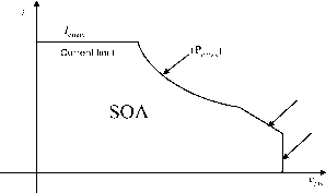 Second breakdown limit Voltage limit CE,max FIGURE 6.23 Safe operation area (SOA) for MOSFET. Drain Gate npn BJT Source FIGURE 6.24 MOSFET equivalent circuit including the parasitic BJT. 1 ... 6 7 8 9 10 11 12 ... 91 |
|
© 2026 AutoElektrix.ru
Частичное копирование материалов разрешено при условии активной ссылки |